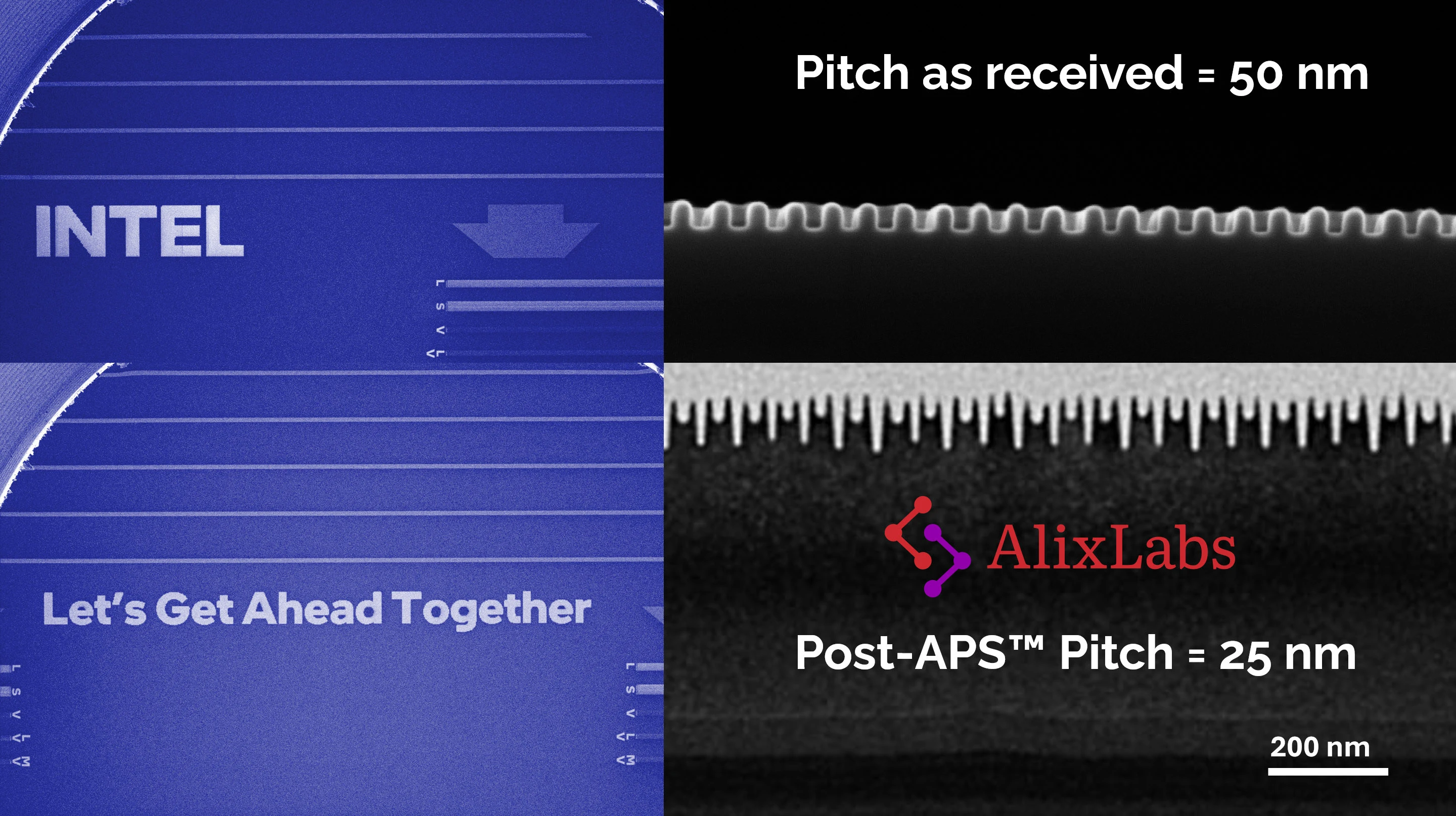
Atomic Layer Pitch Splitting: a breakthrough equipment solution for advanced semiconductor manufacturing.
技術介紹:
Technology Introduction:AlixLabs' unique and patented Atomic Layer Pitch Splitting (APS) is a novel plasma-based etching method that selectively targets surface topology. This breakthrough technology eliminates several complex steps in chip manufacturing, enabling more efficient, cost-effective, and sustainable semiconductor production.
Industry Applicability:
APS enables cost-efficient scaling of semiconductor devices by doubling pattern density. It reduces manufacturing costs, lowers energy use, and supports sustainable, high-volume production. Applicable in logic, memory, and power devices, APS accelerates industrial adoption with scalable chip manufacturing.
產業應用性:
-
AlixLabs AB
"AlixLabs is a Swedish semiconductor industry supplier with equipment and processes capable of manufacturing nanostructures with characteristic sizes smaller than 20 nanometers.
We enable energy efficient fabrication of structures beyond the resolution limits of optical and electron beam lithography – through APS™."
We enable energy efficient fabrication of structures beyond the resolution limits of optical and electron beam lithography – through APS™."
其他資訊
展館別:未來科技館 FK20
所屬部會/單位:國家科學及技術委員會
主要應用領域:材料化工與奈米
更多資訊
展館別:未來科技館 FK20
所屬部會/單位:國家科學及技術委員會
主要應用領域:材料化工與奈米
專利資訊:
16084992