Atomic Layer Pitch Splitting: a breakthrough equipment solution for advanced semiconductor manufacturing.
Technology Introduction:
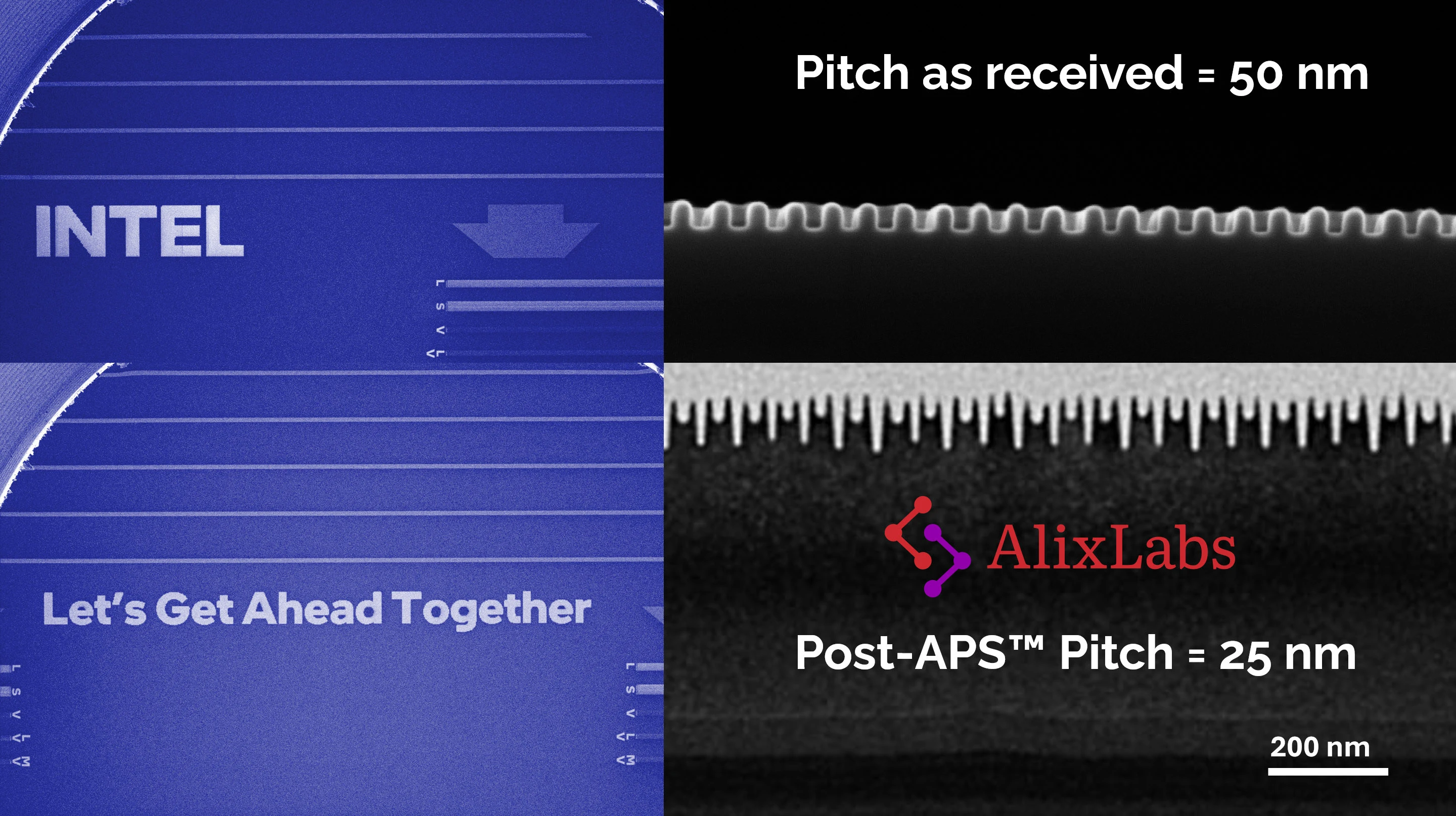
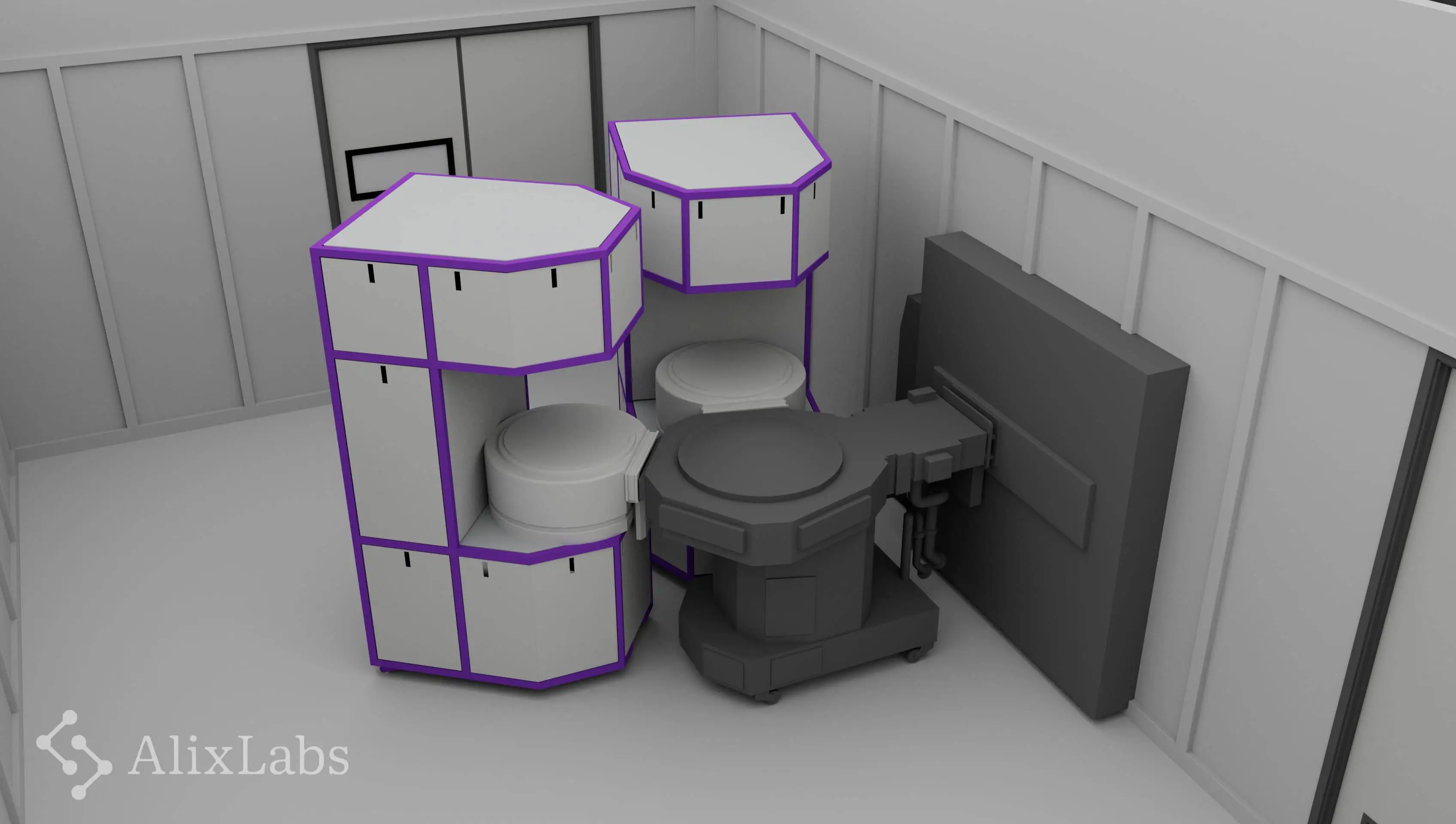
Technology Introduction:AlixLabs' unique and patented Atomic Layer Pitch Splitting (APS) is a novel plasma-based etching method that selectively targets surface topology. This breakthrough technology eliminates several complex steps in chip manufacturing, enabling more efficient, cost-effective, and sustainable semiconductor production.
Industry Applicability:
APS enables cost-efficient scaling of semiconductor devices by doubling pattern density. It reduces manufacturing costs, lowers energy use, and supports sustainable, high-volume production. Applicable in logic, memory, and power devices, APS accelerates industrial adoption with scalable chip manufacturing.
Industrial Applications:
-
AlixLabs AB
"AlixLabs is a Swedish semiconductor industry supplier with equipment and processes capable of manufacturing nanostructures with characteristic sizes smaller than 20 nanometers.
We enable energy efficient fabrication of structures beyond the resolution limits of optical and electron beam lithography – through APS™."
We enable energy efficient fabrication of structures beyond the resolution limits of optical and electron beam lithography – through APS™."
Additional Information
Pavilion:Future Tech FK20
Exhibiting Entity:National Science and Technology Council
Application Category:Materials, Chemical Engineering and Nanotech
More
Pavilion:Future Tech FK20
Exhibiting Entity:National Science and Technology Council
Application Category:Materials, Chemical Engineering and Nanotech
Patents:
16084992