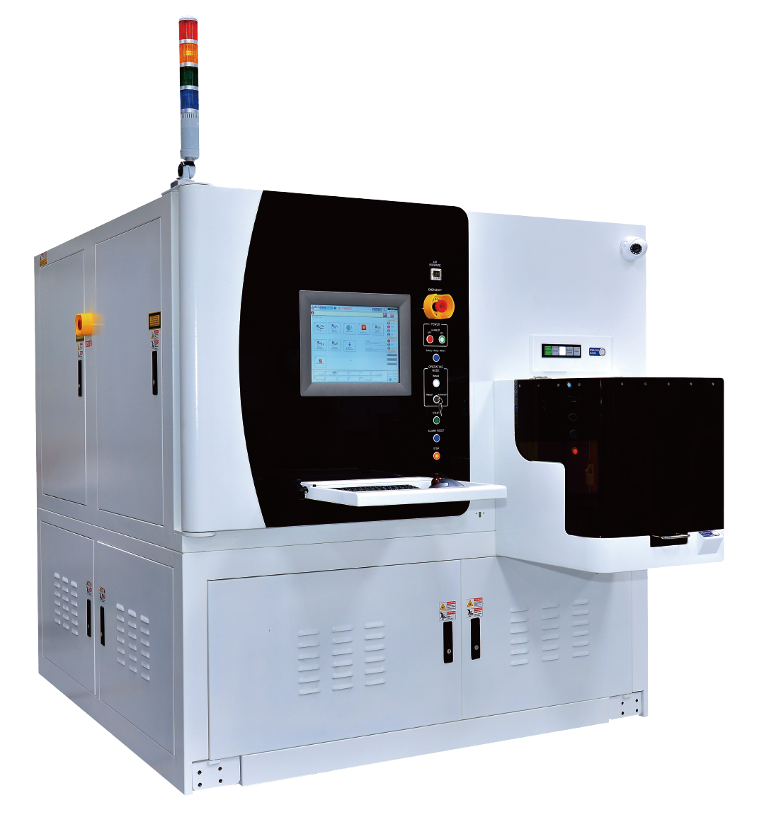
When chips are becoming smaller and thinner, wafer dicing is facing challenging such as increasing material loss due to the width of the dicing lane, mechanical or heat-induced damage to the dies and increasingly longer processing times due to line-by-line sequential dicing. Plasma wafer dicing is an attractive solution to overcome the above challenges in terms of quality and throughput.
Building integrated management system by artificial intelligence based on big data analysis and data mining to implement precision medicine in healthcare management
A 400-Gb/s Ultra-High-Speed Bidirectional FSO Communication for Cloud Server Data Transmission/Switching
Big Data Analytic Module for Key Interval Definition and Indicator Extraction using Equipment Sensor Profile
An extensive intelligent video surveillance system for community-based disaster prevention application
Technology maturity:Mass production
Exhibiting purpose:Product promotion
Trading preferences:Negotiate by self
Coming soon!