
A method for detecting a two-dimensional material is provided. In the method, a suitable OM image from a cloud database is converted into a space spectral data by a hyper spectral imaging technology of visible light and a Raman data of a grown layer number and a grown position of a sample are used as a label of data set, and the space spectral data and the label are used as an input of a model with 3D-CNN.A method for detecting a two-dimensional material is provided. In the method, a suitable OM image from a cloud database is converted into a space spectral data by a hyper spectral imaging technology of visible light and a Raman data of a grown layer number and a grown position of a sample are used as a label of data set, and the space spectral data and the label are used as an input of a model with 3D-CNN.With the superior performance of two-dimensional (2D) materials and its wafer-level synthesis methods, it has attracted more and more attention, aroused great interest and triggered a revolution in the application of corresponding devices. However, the large-scale characterization, accuracy, intelligent automation and high-efficiency detection of nanostructures for two-dimensional materials have not yet been successfully applied at industrial level. It can be applied to semiconductor industry, display, photoelectric material industry.
National Chung Cheng University is a national university in Minxiong Township, Chiayi County, Taiwan. CCU is a member of the Association to Advance Collegiate Schools of Business.
Name:王祥辰
Phone:05-2720411#33601
Address:No.168, Sec. 1, University Rd., Minhsiung Township, Chiayi County 621, Taiwan (R.O.C.)
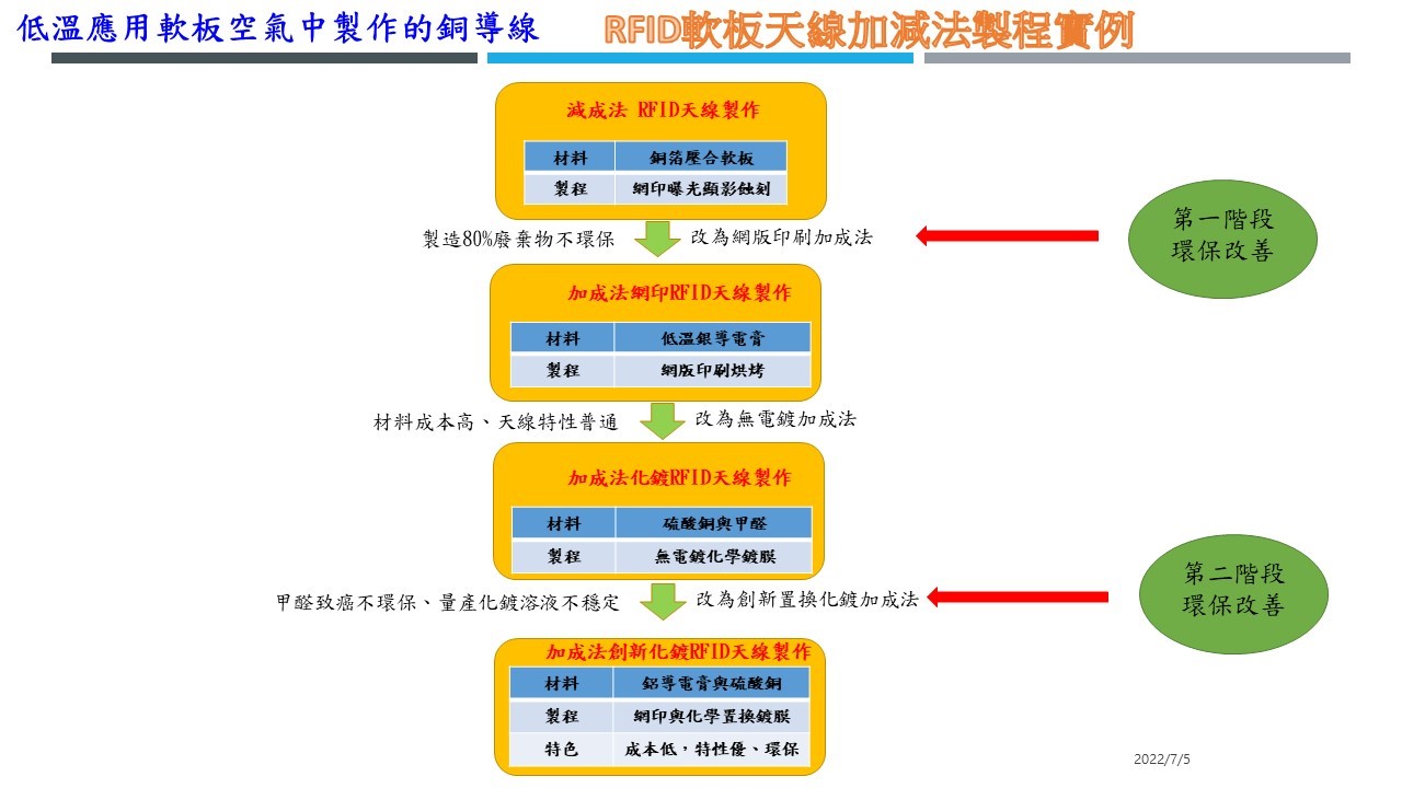
Utilization of novel chemical displacement environmental protection coating technology to be applied on RFID antenna production
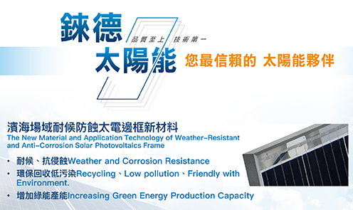
The new material and application technology of weather-resistant and anti-corrosion solar photovoltaics frame in coastal field
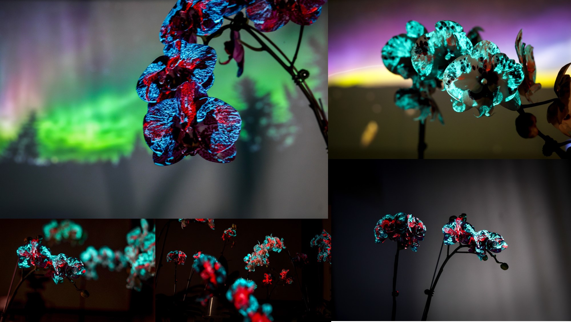
Luminous Aurora Orchid Controlled High Entropy Materials in Indoor Carbon Reduction Technology
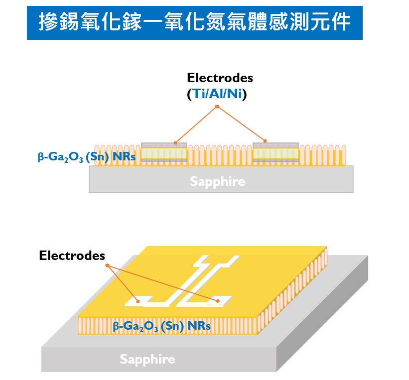
A novel high-performance Sn-doped gallium oxide thin-film nitric oxide gas sensor for applications in smart healthcare and environmental monitoring
Technology maturity:Prototype
Exhibiting purpose:Technology transactions、Patent transactions、Product promotion、Display of scientific results
Trading preferences:Exclusive license/assignment、Technical license/cooperation、Negotiate by self
*Organization
*Name
*Phone
*Main Purpose
*Discuss Further
*Job Category
*Overall Rating
*Favorite Area
*Key Tech Focus
*Willing to Receive Updates?
Other Suggestions
Coming soon!