METHOD OF TRANSFERRING NANOSTRUCTURES AND DEVICE HAVING THE NANOSTRUCTURES
Devices with physical flexibility and stretchability have attracted a great deal of interest for use in wearable electronic technology and large-area electronics, including displays, energy harvesters, energy storage devices, distributed sensor networks, and Internet of Things applications. Single-crystal III-nitride nanorods and two dimensional transition metal dichalcogenides (2D TMDs) are one of the most important semiconductors due to their tunable and direct band gap, good chemical stability, tunable electrical structure, and great piezoelectrical characteristics for a large number of applications, such as piezoelectric nanogenerators, nanolasers, photodetectors, photovoltaic cells, and hydrogen generation. High-quality crystalline III-nitride nanorods and 2D TMDs are typically epitaxied at high temperatures on rigid single-crystalline Si (111), sapphire, and SiC substrates, but these substrates cannot be adapted for flexible electronics or some applications.
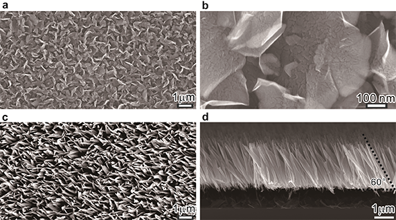
To overcome the problems from the conventional substrates, an efficient approach for growing and transferring wafer-scale of high density single-crystalline GaN NRs by MOCVD method using the innovative 2D materials, defective 2D graphene and 3D graphene (or called vertically oriented graphene (VG) nanosheets), was provided. Previous results have been demonstrated that the defective 3D graphene can be used for fabricating transparent flexible devices embedded within the transferred obliquely aligned GaN NRs grown by MBE method. Moreover, the wafer-scale defected 2D graphene has similar defect structures with the 3D graphene but providing an ultra uniform surface morphology (ultra thin thickness (1 nm) and ultra smooth surface (Rq 0.15 nm)) compared to the 3D graphene, which is more applicable for conventional semiconductor fabrication process. The 2D graphene developed in this work could be an excellent platform to epitaxy and transfer high-quality II-VI and III-V nanostructures for flexible and three-dimensional stacked electronics.
An illustrative method for transferring nanostructures is provided with the steps of: forming a two-dimensional material (2D material) (the innovated 2D graphene or 3D graphene) on a first substrate; forming a plurality of nanostructures on the 2D material; bonding a surface of one or more of the plurality of nanostructures with a head or a second substrate, and/or shaking the one or more nanostructures with or without a fluid; and separating the one or more nanostructures from the 2D material for flexible device, microLED, and 3DIC applications.
線上展網址:
https://tievirtual.twtm.com.tw/iframe/b84b38e1-5c39-4398-b104-4d3fa37b9bc6?group=23bfb1fa-dd5b-4836-81a1-4a1809b1bae5&lang=en
The main missions of NIAR are: To establish R&D platforms To support academic research To promote frontier science and technology To foster high-tech talent
COMPOSITE WITH MULTI-DIMENSIONS HOLLOW STRUCTURES AND APPLICATION THEREOF
ORGANOMETALLIC IRIDIUM COMPLEX, SYNTHETIC METHOD THEREOF, AND ORGANIC LIGHT EMITTING DEVICE USING THE SAME
CARBON FIBER STOVE RACK STRUCTURE AND THE METHOD OF MANUFACTURING THE SAME
POLYMERIC BENZOXAZINE RESIN STRUCTURE WITH ADAMANTANE-CONTAINING MAIN CHAIN
Technology maturity:Experiment stage
Exhibiting purpose:Technology transactions、Product promotion、Display of scientific results
Trading preferences:Exclusive license/assignment、Technical license/cooperation、Negotiate by self
*Organization
*Name
*Phone
*Main Purpose
*Discuss Further
*Job Category
*Overall Rating
*Favorite Area
*Key Tech Focus
*Willing to Receive Updates?
Other Suggestions
Coming soon!