Technology Introduction:
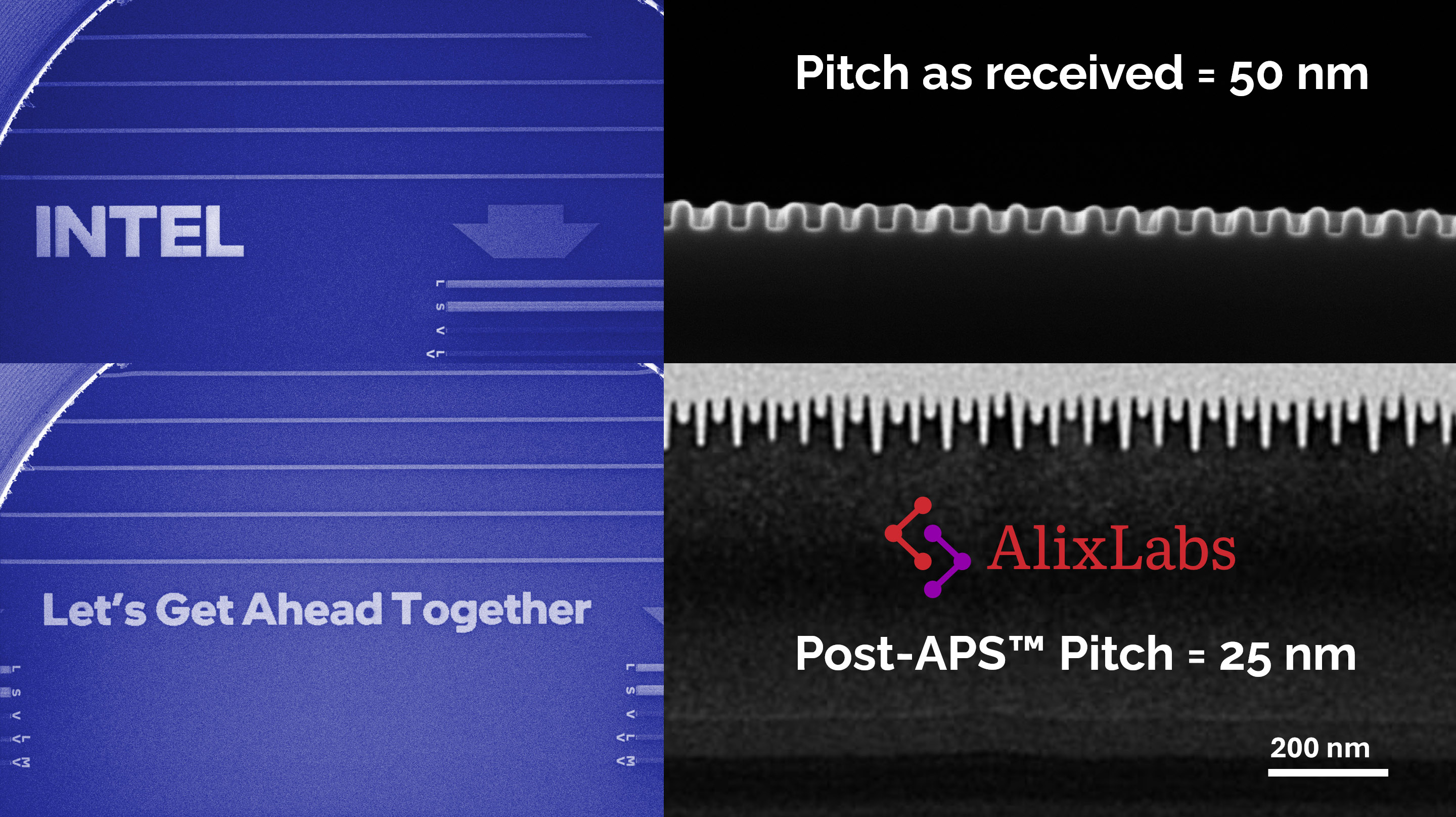
AlixLabs' unique and patented Atomic Layer Pitch Splitting (APS) is a novel plasma-based etching method that selectively targets surface topology. This breakthrough technology eliminates several complex steps in chip manufacturing, enabling more efficient, cost-effective, and sustainable semiconductor production.
Industry Applicability:
APS enables cost-efficient scaling of semiconductor devices by doubling pattern density. It reduces manufacturing costs, lowers energy use, and supports sustainable, high-volume production. Applicable in logic, memory, and power devices, APS accelerates industrial adoption with scalable chip manufacturing.
"AlixLabs is a Swedish semiconductor industry supplier with equipment and processes capable of manufacturing nanostructures with characteristic sizes smaller than 20 nanometers. We enable energy efficient fabrication of structures beyond the resolution limits of optical and electron beam lithography – through APS™."
16084992
Materializing a sustainable future through innovative thermal management
First-of-its kind super-absorptive non-drugs-based lenses to treat eye infections and chemical eye injuries.
UV Excimer Cure - Matting Technology for Matte and Resistant Flooring
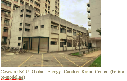
NCU-Covestro Research Center: Research and Development of Green Advanced Functional Materials and Manufacturing Processes
技術成熟度:雛型
展示目的:商機推廣
流通方式:新產品開發
*服務單位
*姓名
*電話
*您參觀這項展品的主要目的?
*您是否希望進一步洽談
*您的職務類別
*展覽整體評價
*最喜歡的展區
*期待展覽著重的技術領域
*是否願意收到電子報/最新資訊
其他建議
敬請期待!