AI-Semi : A platform for Intelligent Optimization in Semiconductor Device Designs, Manufacturing, and Performance
In order to accelerate the device optimization and improve the device characteristic prediction, AI-based approach with using the neural network is developed. Based on the semiconductor device development process, a large amount of design, manufacturing and measurement parameter data is generated. Therefore, these experimental data can be used in conjunction with machine learning to build an artificial intelligence engine. Semiconductor device design, manufacturing and characteristic optimization platform developed by AI technology is able to integrate previous technological results to predict the future device technology characteristics with an accurate analysis of the complex parameters to optimize the device performances, which can help to reduce the cost and time for the development.“AI-Semi”can accelerate the optimization of the semiconductor devices toward the targeted performance.
1. Machine learning engine to accelerate the device modeling and designs
Our platform can model the electrical characteristics and reliability in advanced technologies, which are the challenges for the physics-based models. In addition, based on the developed machine learning engines, our platform can predict the electrical characteristics.
2. Autoencoder to reconstruct the device parameters based on the target performance
Considering the following targeted performance: VTH(V)=.014V, SS(mV/dec)=98, ID_Max(mA/mm)=0.025 and ID_OFF(mA/mm)=3.6×10-12, the required device designs, which are (tAlGaN, Lg, Recessed depth)=(10.3nm, 1.47μm, 4.9nm), can be obtained by using the autoencoder.The conventional method of optimizing the performance is a time-consuming process that requires a lot of resources. For the devices based on the novel materials and designs, the lack of accurate physics-based models results in a challenge to predict the device characteristics, leading to the uncertainties of product performance. Our platform can be used in a variety of complicated semiconductor technologies to achieve an accurate analysis of the key designs and processing parameters, further efficiently optimizing device characteristics and reliability. This platform can significantly reduce the cost, time and resources in the post-Moore era, providing the useful assistance in More Moore (such as sub-10nm beyond CMOS) and More than Moore (such as power semiconductor devices) technologies.
Big Data Analytic Module for Key Interval Definition and Indicator Extraction using Equipment Sensor Profile
The Development of the Software and Hardware to the Internet of Additive Manufacturing System based on Vat Photopolymerization Technology.
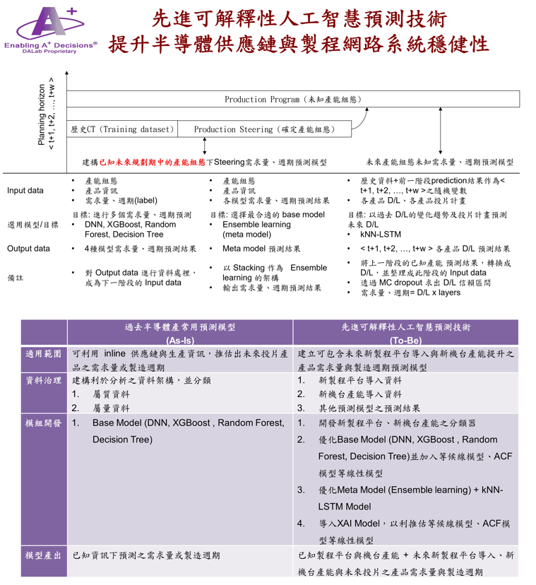
Advanced artificial-intelligence based forecasting technique to enhance semiconductor supply chain and manufacturing network resilience

"1) Integrating AI recognition, IoT, and blockchain into traceable software and hardware for recycling UCO 2) Cutting-edge 3D learning platform powered by Spatial AI 3) Optimize use of existing buildings by making them transformable and adaptive to human needs at the click of a button 4) Non-contact image analysis and calculation technology to capture vital signs through dynamic face detection"
Technology maturity:Prototype
Exhibiting purpose:Technology transactions、Product promotion、Display of scientific results
Trading preferences:Technical license/cooperation
Coming soon!