Industrialized synthesis technique of high quality and ultra-large area graphene

In this technique, we develop batch to batch chemical vapor deposition (B2B-CVD) method to reduce the cost to facilitate the industrial production. In R2RCVD, in order to grow large-scale graphene in a more economic route by typucal furnace tube, the rolling of copper foils combined with quartz scaffold and isolation layer can overcome the issue of adhesion between Cu foils when it was subjected to high temperature growth. This invention provides a effective and novel method that can produce ultra-large graphene film with high-quality. It adopts simple operation and economic reaction components to increase the output of batch production of graphene to meet the demaned of industrialization and marketing.The equipment of roll-to-roll technology for growing large-area graphene developed by Samsung or Sony is expensive and the control of parameters must be very precise.
The breakthrough of our technology is that the existing equipment is used to obtain the most effective synthetic area. The high-density winding and batch to batch method with the special insulating layer proposed by our technology can be used to grow graphene on a large scale and has good quality. The sheet resistance is about 750 Ω/sq, the defect density is about 2.43×1012 cm-2. When the furnace tube diameter reaches 8 inches, the yield can be increased from 5.3 m2/h (reported in the literature of roll-to-roll method) to 6.7 m2/h.1. Graphene has high light transmittance (light transmittance of single-layer graphene is 97%), high thermal and electrical conductivity and flexibility, which is suitable for ultra-high transparent conductive film.
2. Single layer graphene is quite sensitive to the change of surface charge transfer, and the surface is also easy to be chemically modified. It can be combined with circuit design to develop biosensor device with extremely high sensitivity.
3. The transfer of large-area graphene to the silicon substrate can enhance the epitaxial growth of GaN to on its surface and be applied to specific niche electronic devices.
Name:蘇清源
Phone:03-4227151#34911
Address:No. 300, Zhongda Rd., Zhongli District, Taoyuan City
Innovative valorization of non-hazardous oily sludge for the production of fuel oil and mesoporous magnetic carbon composite materials
Novel and green process to synthesis high quality graphene as conductive additives for Li ion batteries

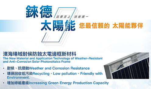
The new material and application technology of weather-resistant and anti-corrosion solar photovoltaics frame in coastal field
.png)
Green & Continuous Manufacturing, a novel integrated liquid-liquid micro-extractor and separator for rapid downstream process characterization.
Technology maturity:Prototype
Exhibiting purpose:Technology transactions、Patent transactions、Product promotion、Display of scientific results
Trading preferences:Exclusive license/assignment、Technical license/cooperation、Negotiate by self
Coming soon!