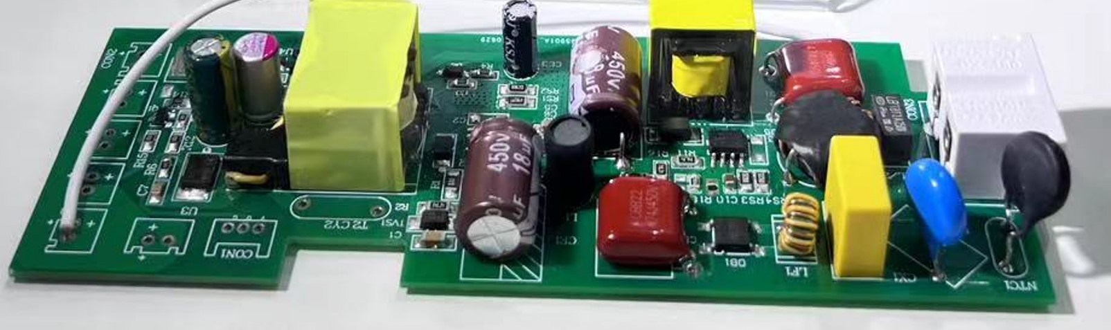
The epitaxial layer structure of the GaN-on-Si substrate was improved, and the HEMT device fabrication process was optimized to achieve a GaN HEMT device with a breakdown voltage of >1200V
學研單位
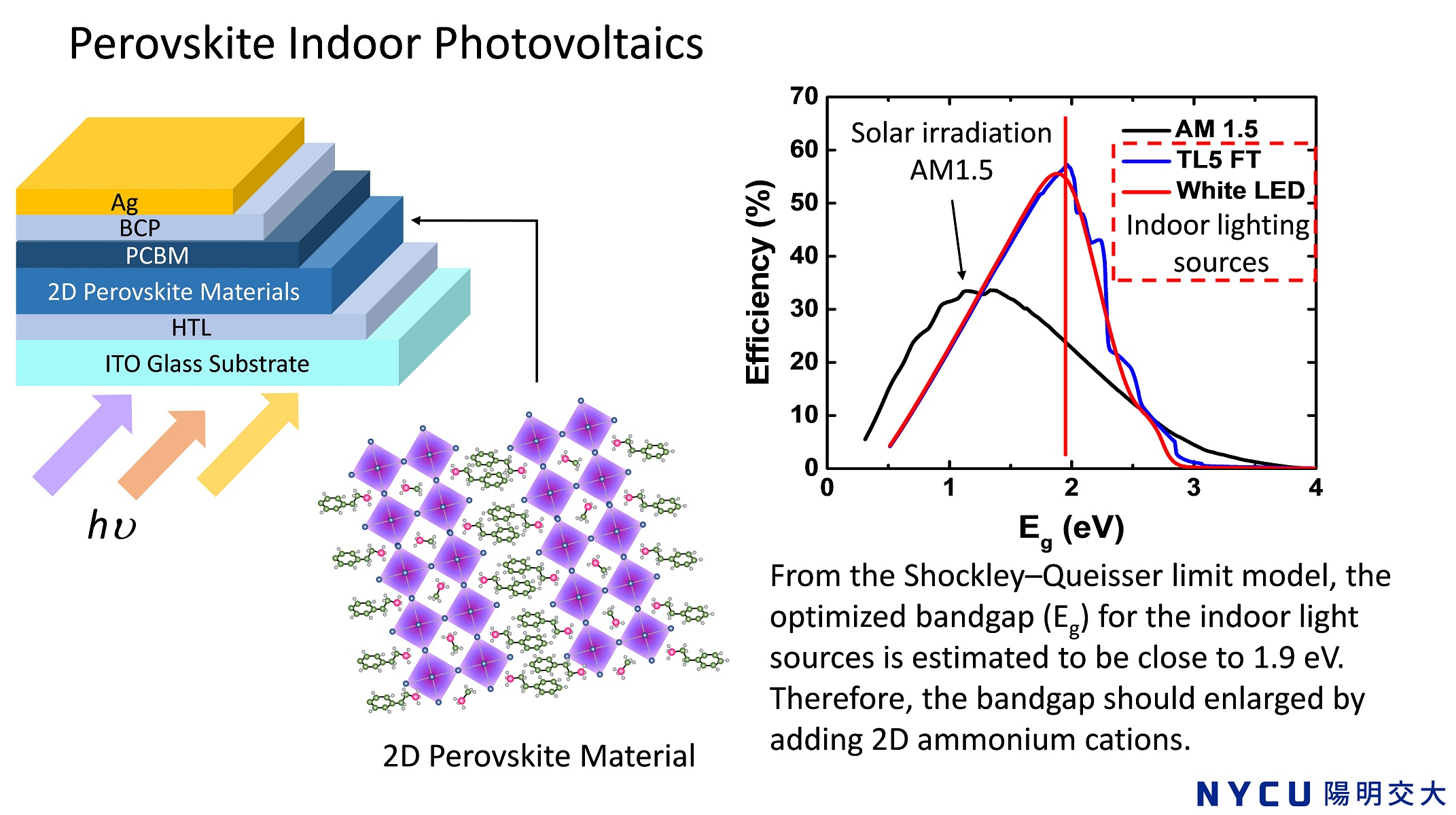
Emerging Two-Dimensional Perovskite Indoor Photovoltaics for Children Healthcare System Based on Internet of Things Technologies
Shooting color measurement system and image color cloud processing service platform

High temperature and corrosion resistant SiC susceptor for compound semiconductor process
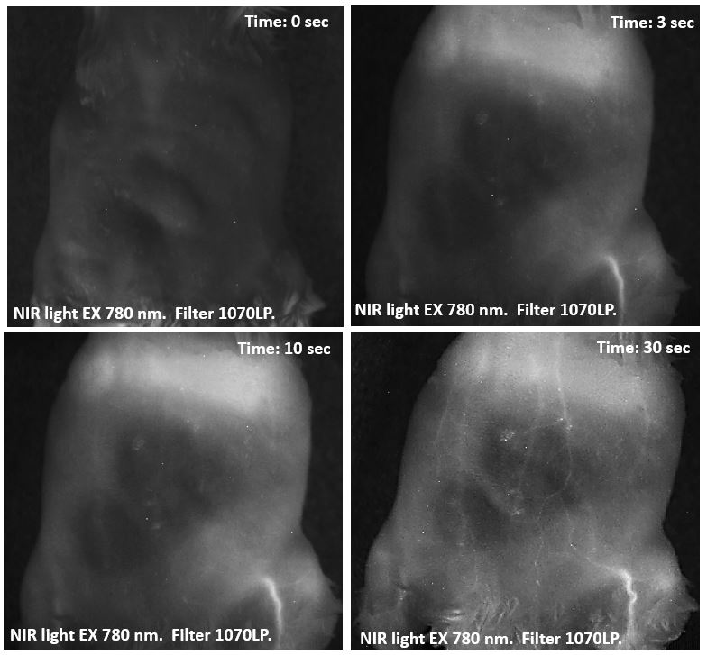
High-brightness fluorescent gold nanoclusters infrared imaging agent technology with clinical application potential
Technology maturity:Experiment stage
Exhibiting purpose:Display of scientific results
Trading preferences:Negotiate by self
Coming soon!