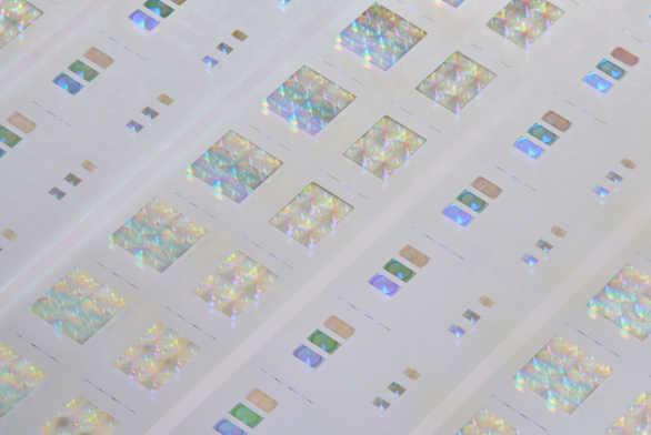
Develops high-performance, ultra-thin metalenses for next-generation optical applications. These semiconductor lenses replace traditional bulky optics with nanostructured, flat-surface alternatives that offer reduced size and weight while maintaining or enhancing performance. Through strategic collaborations with A*STAR institutes, MetaOptics has developed scalable processes such as Direct Laser Writing and 300mm wafer-level metasurface fabrication.
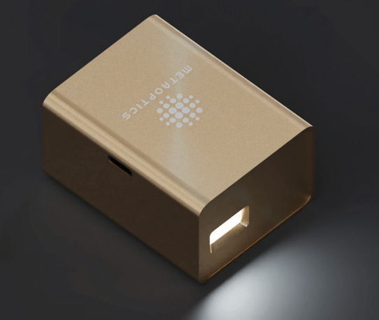
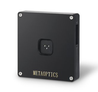
MetaOptics metalenses are applicable across multiple industries including consumer electronics (smartphones, AR/VR), IoT cameras, automotive LiDAR, biometric authentication, and compact projection systems. Our pico projectors and color cameras serve emerging markets in AI-powered imaging, while our scalable manufacturing enables cost-effective integration into high-volume products.
At Metaoptics Technologies, we are breaking through current lens limitations in consumer and IoT applications. Our high-throughput meta lens production ensures efficiency and cost-effectiveness. As AR/VR and HUD technologies rapidly expands, our innovative meta lens are essential to provide miniaturization in supporting this market growth.
Name:Egor Khaidarov
Phone:+65 82102353
Address:81 Ayer Rajah Crescent 01-45 Singapore 139967
20190257986
The innovative technology that turns waste into treasure – Silicon Dioxide regenerated from semiconductor waste that contains Silicon
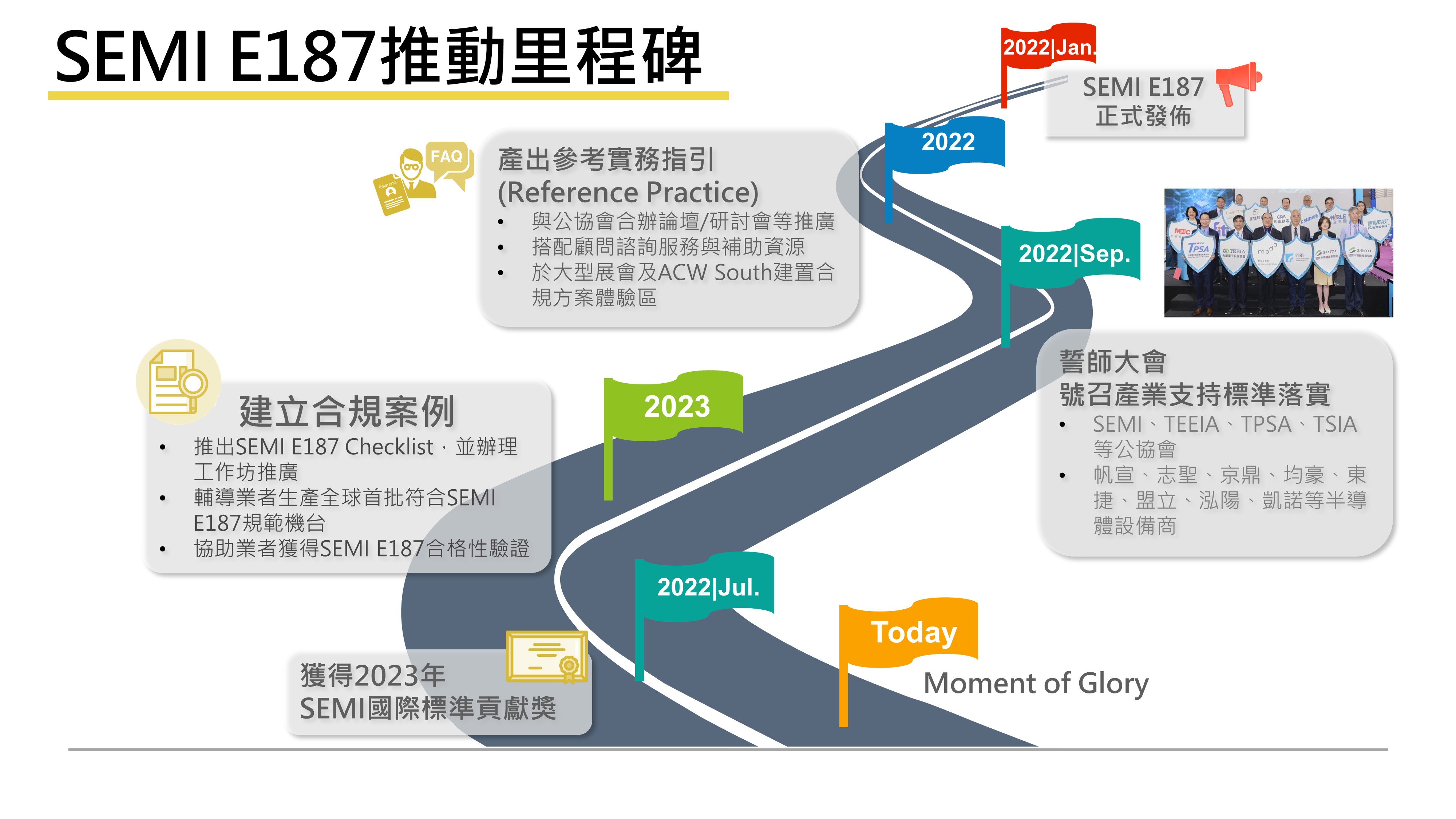
SEMI E187-Specification for Cybersecurity of Semiconductor Fab Equipment
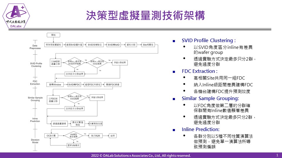
Optimizing Advanced Process Control Decision and Virtual Metrology Technology for Nano Technology Nodes for Semiconductor Manufacturing
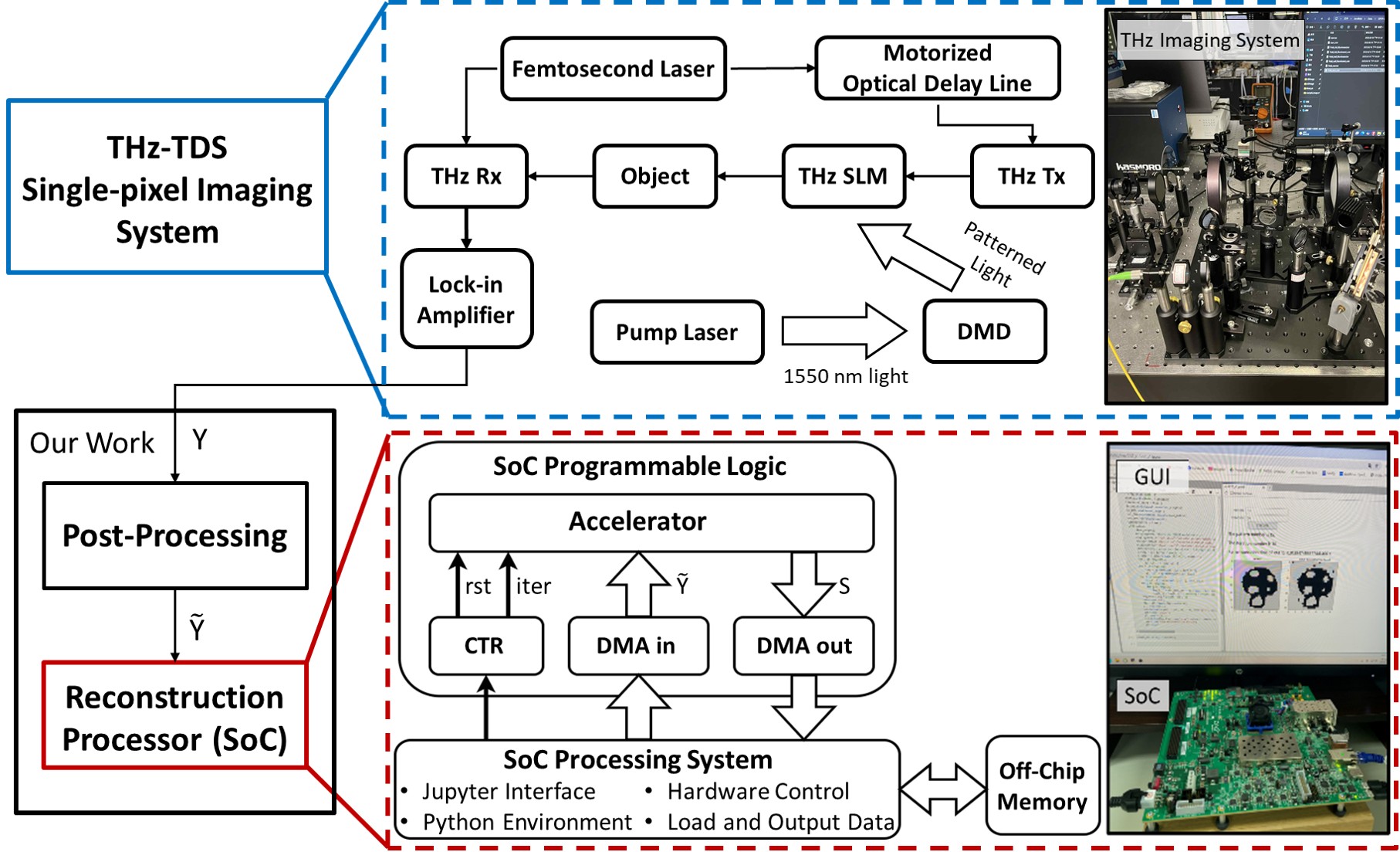
Terahertz Single-Pixel Imaging SOC System for Semiconductor Material Analysis
Technology maturity:Mass production
Exhibiting purpose:Product promotion
Trading preferences:Negotiate by self
*Organization
*Name
*Phone
*Main Purpose
*Discuss Further
*Job Category
*Overall Rating
*Favorite Area
*Key Tech Focus
*Willing to Receive Updates?
Other Suggestions
Coming soon!