Novel Monolithic 3D Heterogeneous Semiconductor Device Integration f or Ultra-High-Density (20M NAND-Gate/mm^2) Logic Gate Circuits
The aim of this proposed technology is to develop a Novel Monolithic thr
ee-dimensional (M3D) Heterogeneous Semiconductor Device Integration
for Ultra-High-Density Logic Gate Circuits, achieving a density of over 20
million NAND-Gates per square millimeter. This will be accomplished thro
ugh the utilization of high-performance stacked field-effect transistors, o
vercoming the challenges associated with integrating heterogeneous sem
iconductor devices and realizing ultra-high-density logic circuit technolog
ies. The research will encompass various aspects, including novel semicon
ductor materials, high-efficiency and low-power transistors, process integ
ration, and logic gate circuit implementation.
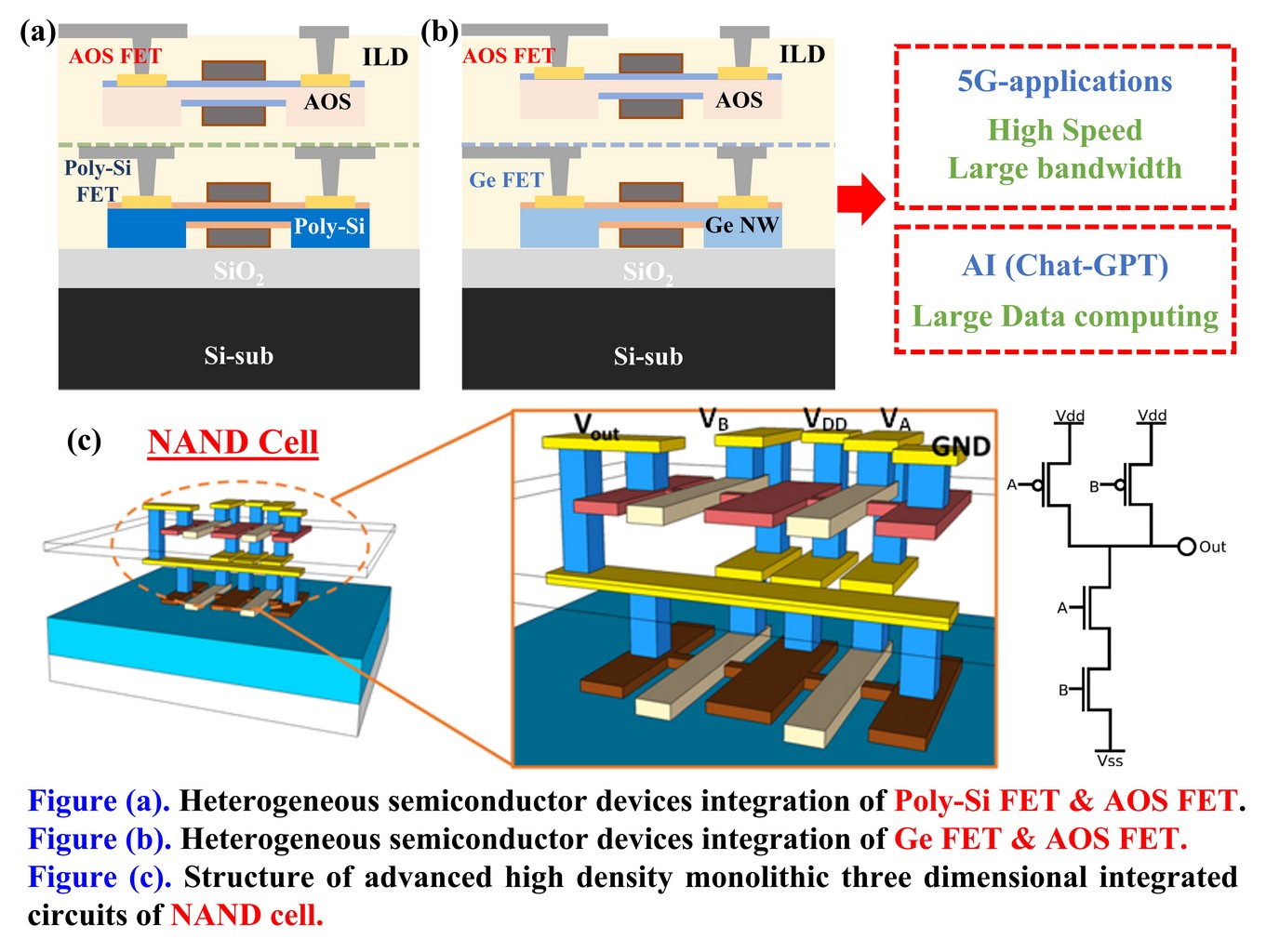
Two types of advanced device 3D-stacking technologies will be develope
d. Gate-all-around (GAA) single-crystal germanium nanosheet transistors
and polycrystalline silicon thin-film transistors will act as the first layer of
high-performance transistor devices. Subsequently, the high-performanc
e GAA indium oxide (InOx)-based nanosheet transistors with low thermal
budget will be stacked on top of the aforementioned first-layer transistor
s, forming the second layer of low-power transistor elements and constru
cting the monolithic 3D-IC (M3D-IC) architecture. This approach effectivel
y enhances the integration density of transistors within a single chip. To ac
hieve the objective of high-density logic gates, specifically NAND gates, o
ur focus will be on the 3D heterogeneous integration of n-channel TFT an
d p-channel TFT for implementing NAND logics. The goal is to realize a N
AND logic circuit with a density of 20M NAND-Gate/mm^2, which corres
ponds to approximately 80 million transistor devices within a 1mm2 area.
It is important to note that there have been no reported research findings
on high-density NAND architecture utilizing monolithic 3D-IC technology,
highlighting the innovative nature of our proposed technologies.
National Yang Ming Chiao Tung University (NYCU) was formed in 2021 through the merger of National Yang Ming University and National Chiao Tung University. Located in Hsinchu, Taiwan, NYCU is a leading institution specializing in technology, engineering, medicine, and social sciences. The university is known for its strengths in research and innovation, particularly in areas such as information technology, biomedicine, and artificial intelligence. NYCU fosters interdisciplinary collaboration, global partnerships, and aims to nurture professionals with strong academic foundations and leadership skills to address societal challenges and contribute to technological advancements.
Intelligent IoT Cloud and Autonomous Vehicular Techniques for Efficient Integration of Heterogamous Manufacturing Equipment
Algorithm-Driven Design: Using new algorithm and deep learning model to control the microstructures generation of favorable mechanical behavior (Static & Dynamic) in additive manufacturing.
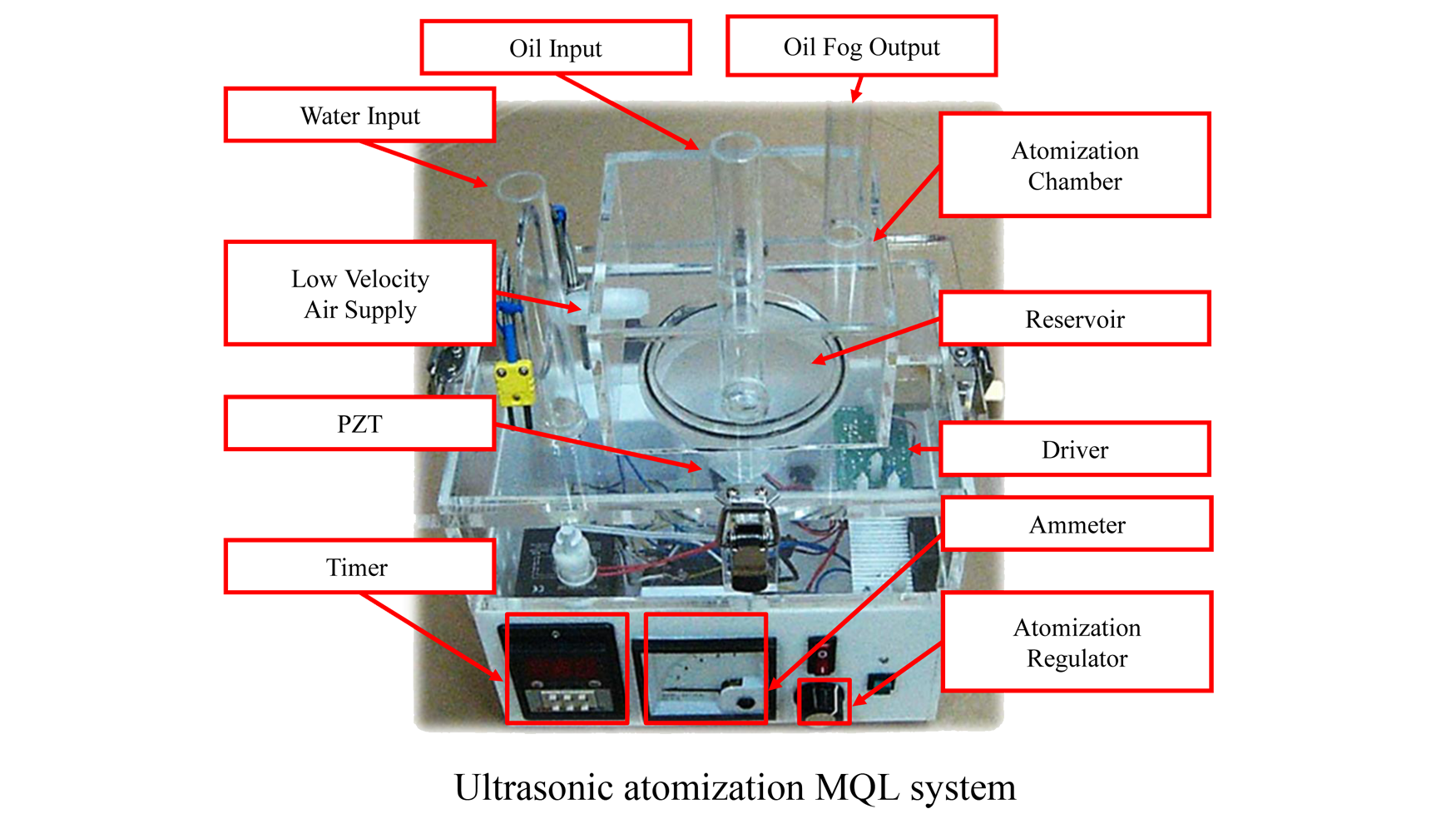
Nanofluid/ultrasonic atomization micro-lubrication system development and application intelligent modeling method to improve the multiple quality characteristics of the micro-machining process research and optimal prediction model establishment
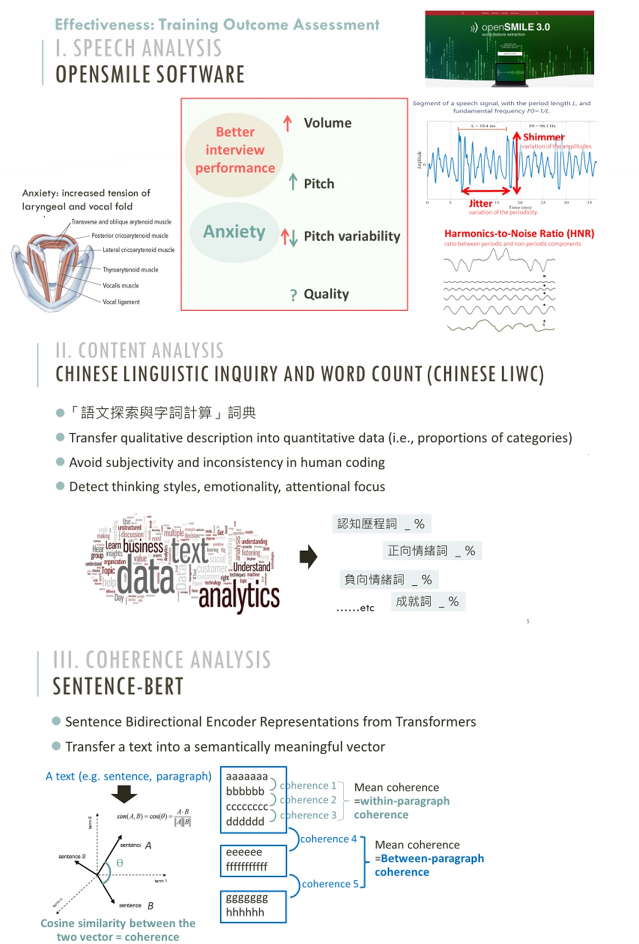
Targeting job interview and workplace communication skills for autistic adults: An innovative cognitive-behavior therapy-based virtual reality intervention program
Technology maturity:Concept
Exhibiting purpose:Display of scientific results
Trading preferences:Negotiate by self
Coming soon!