
Regarding β-Ga2O3 epi-wafers and substrates for power devices, Novel Crystal Technology, Inc. is the only one manufacturer in the world. Our company possesses the following technologies.
1. Production of large, high-quality β-Ga2O3 single-crystal substrates.
2. Growth of high-purity β-Ga2O3 epitaxial layers.
3. Fabrication of β-Ga2O3 power devices (SBDs, FETs).
β-Ga2O3 has a large band-gap energy, and it can be grown from a melt source. As a result, large, high-quality single-crystal substrates can be manufactured at low cost. These characteristics make β-Ga2O3 a promising material for next-generation power electronics. In fact, β-Ga2O3 is potentially superior to GaN and SiC for power device applications.
預料環境、能源、IT、材料等將成為日本的核心產業,在其關鍵技術之高頻與類比(More than Moore)半導體 相關事業領域創造新產業、加速開放式創新、為日本的產業振興做出貢獻是我們的目的。
姓名:Shutaro Nambu
電話:
地址:102Kujo CID Bldg.13 Higashikujo-shimotonodacho, Minami-ku, Kyoto, 601-8047, Japan
Solar power textile, Laser processing for micro fabrication, and Thin-ply thermoplastic prepreg for CFRP
First-of-its kind super-absorptive non-drugs-based lenses to treat eye infections and chemical eye injuries.
Gallium Oxide (Ga2O3) Substrates and Epitaxial wafers
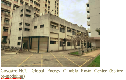
NCU-Covestro Research Center: Research and Development of Green Advanced Functional Materials and Manufacturing Processes
技術成熟度:實驗室階段
展示目的:商機推廣
流通方式:自行洽談
*服務單位
*姓名
*電話
*您參觀這項展品的主要目的?
*您是否希望進一步洽談
*您的職務類別
*展覽整體評價
*最喜歡的展區
*期待展覽著重的技術領域
*是否願意收到電子報/最新資訊
其他建議
敬請期待!