Sub-nanometer Characterization of Semiconductor Transistor Interfaces: Voltage-Tunable Cross-Sectional Scanning Tunneling Microscopy
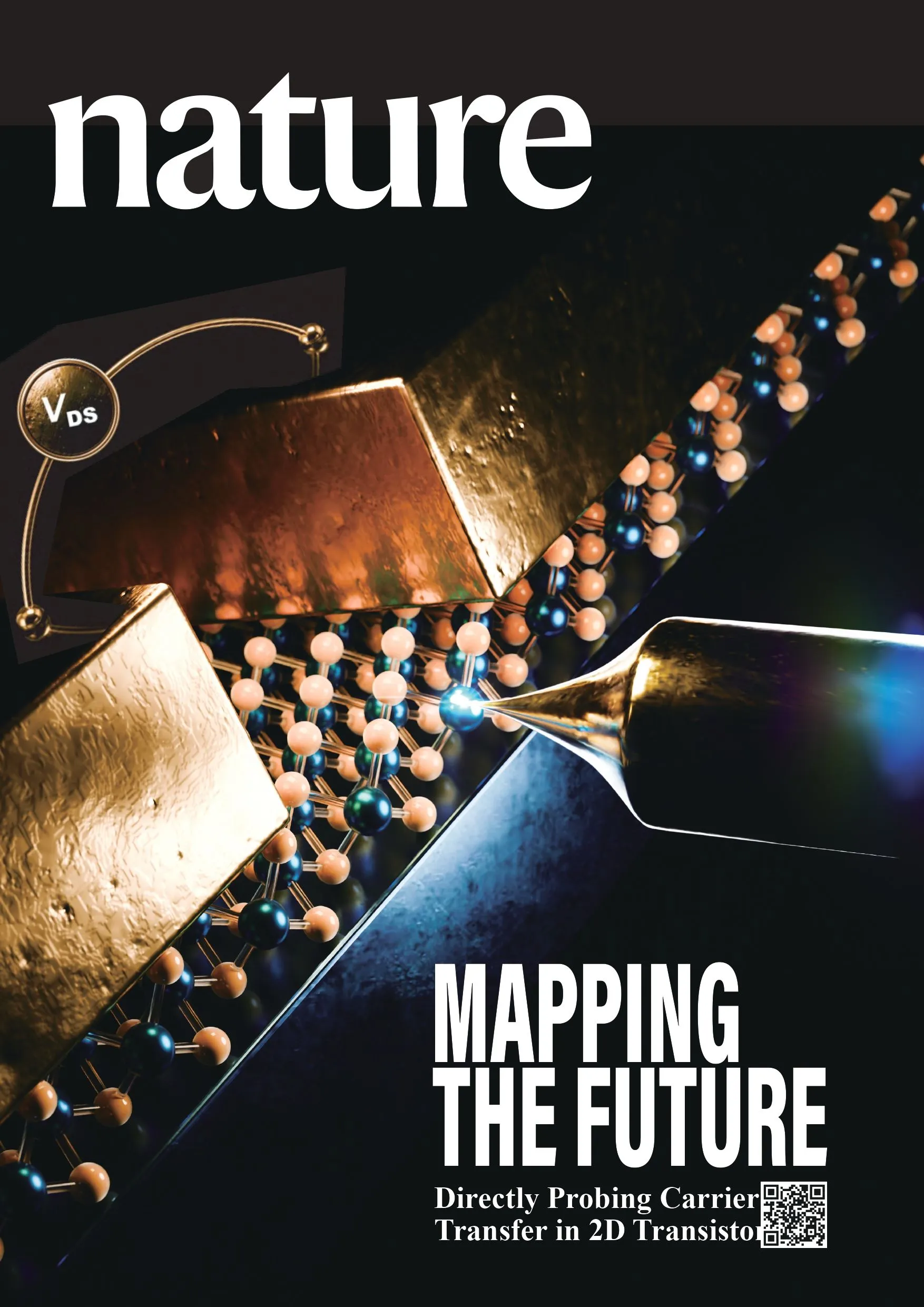
Technology Introduction:
This work presents an in-situ, sub-nanometer-scale electronic characterization of 2D semiconductor devices using cross-sectional STM/STS — a capability previously inaccessible by conventional metrology. By directly imaging carrier injection profiles, electronic structure, and transfer length(LT) at the metal/semiconductor contact with sub-nanometer spatial resolution, this technique uniquely decodes the fundamental physics governing contact scaling limits, offering experimental insight for the advancement of next-generation 2D device technology.
Industrial Applications:
The atomic-scale interfacial characterization capability established here directly addresses the semiconductor industry's most critical challenge at advanced nodes: contact resistance scaling. As 2D semiconductors (MoS₂, WSe₂) emerge as prime successors to silicon technology, metal–semiconductor contact quality has become the key performance bottleneck. This technology delivers the atomic-level physical insights essential for process optimization, material screening, and device design — offering strategic value across leading manufacturers and their equipment and materials supply chains.
National Taiwan University
At present, the University consists of 16 colleges, 58 departments, 146 graduate institutes, as well as 34 Master's and PhD degree programs. NTU's programs cover a wide array of disciplines across science, arts, and the humanities, with up to 8,000 courses made available for selection each semester.
Contact Information
Name:Yan-Ruei Lin
Tel:02-8369-2101
Address:No. 1, Sec. 4, Roosevelt Rd., Taipei 10617, Taiwan (R.O.C.)