Ultra-Weak Light Imaging Technology: Wearable Goggles for Capturing I nvisible Signals


We introduce a groundbreaking infrared imaging technology that combin
es an organic infrared photodetector, a transparent conductive electrode,
and an organic light-emitting diode (OLED) through heterogeneous integr
ation. This integration forms an "organic upconversion device" that exten
ds human perception beyond the visible spectrum, unveiling otherwise in
visible infrared signals. Leveraging the exceptional sensitivity of organic m
olecules to infrared wavelengths, our device converts incident infrared ph
otons into a current flow that emits visible light, utilizing multiple layers of
functional materials. Notably, our approach presents a monolithic infrared
imaging device as an alternative to integrating photodiodes and light-emi
tting diodes using inorganic semiconductor technology. The key features
of our technology include:
1. Disorder characteristic enabling direct contact between heterogeneous
materials.
2. High transparency is achieved by combining the organic molecule's w
avelength selectivity with a semi-transparent conductive electrode.
3. Reduced power consumption due to organic molecules' high sensitivit
y and quantum efficiency, which cover a broad absorption spectrum from
700 to 2000 nm.
4. Solution processing of the active layer allows low-cost deposition over l
arge areas, in contrast to energy-intensive inorganic wafer fabrication.
Leveraging these advantages, we developed a compact wearable glasses-
based infrared imaging technology for in-situ, real-time monitoring, expa
nding human sensing capabilities. This versatile technology finds applicati
ons in various fields, including: (1) addressing privacy concerns, the device
detects and reveals invisible light emitted by infrared cameras, alerting us
ers to potential privacy breaches. (2) Highly sensitive night vision goggles
for military combat deployment.
By harnessing the potential of our innovative technology, we aim to revol
utionize infrared imaging, unlocking new possibilities across di
Ming Chi University of Technology (MCUT; Chinese: 明志科技大學; Pe̍h-ōe-jī: Bêng-chì Kho-ki Tāi-ha̍k) is a private university of technology in Taishan District, New Taipei, Taiwan. Established in 1963, it currently consists of three colleges: College of Engineering, College of Environment and Resources, and College of Management and Design.

World-class ultra-precision optical processing technology and the non-contact floating display application

Ultra-thin Quantum Dots LED packaging technology development program for display application

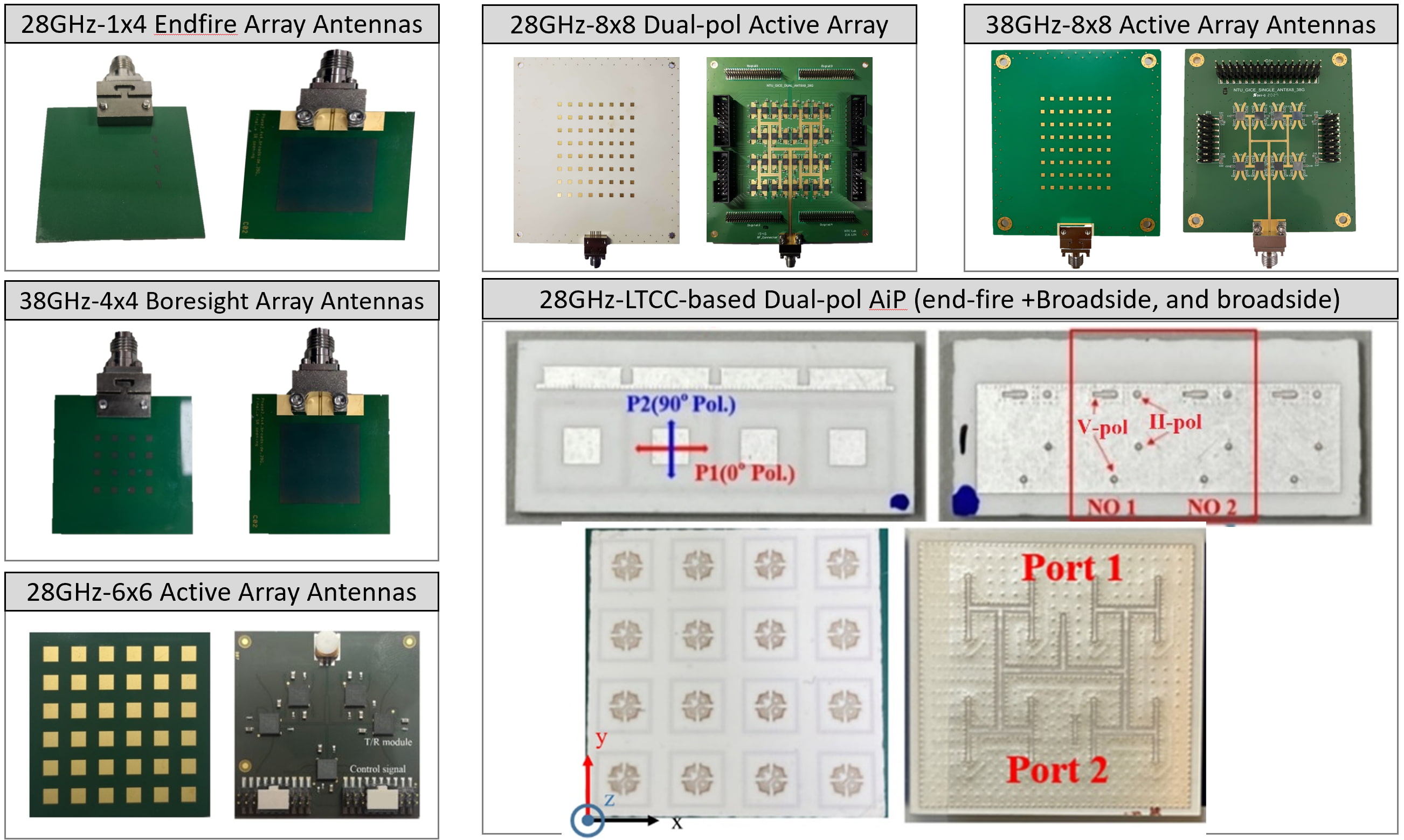
Antenna-in-package (AiP) Technology Suitable for Feeding to the Smart Impedance Material for High-Gain Radiations at Millimeter Wave Frequencies

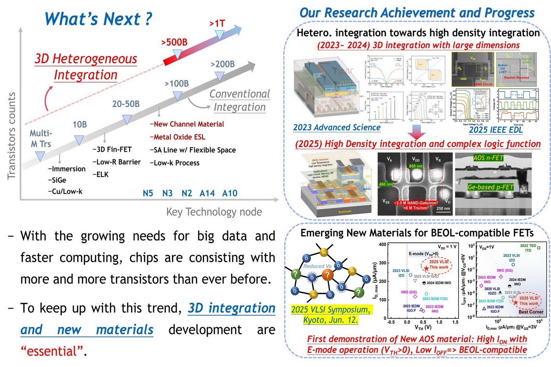
Monolithic 3D Heterogeneous Device Integration and Innovative Materials for Breaking Logic Density Limits: A Key Technology Platform for High-Density AI Computing Chips
Technology maturity:Experiment stage
Exhibiting purpose:Display of scientific results
Trading preferences:Negotiate by self
*Organization
*Name
*Phone
*Main Purpose
*Discuss Further
*Job Category
*Overall Rating
*Favorite Area
*Key Tech Focus
*Willing to Receive Updates?
Other Suggestions
Coming soon!