Ultra-thin Quantum Dots LED packaging technology development program for display application
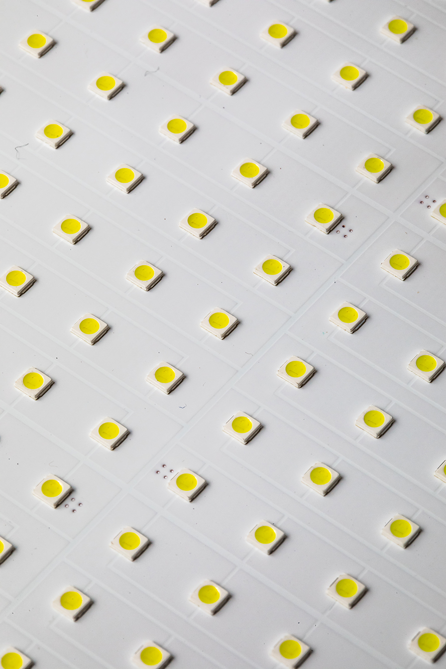
This technology development proposes an ultra-thin LED display that combines ultra-wide color gamut performance and HDR technology. In order to achieve this unique technical feature, Lextar especially developed the ultra-thin Quantum Dots LED packaging technology, named U-Light.
Lextar analyzed the optics and efficiency of LED, minimized the light source design with a special optical lens made the thickness of the backlight module below 10mm which is the first direct LED backlight module to realize ultra-thin display (<10 mm) and ultra-wide color gamut (BT. 2020 >90%) package in the world.
Ultra Thin Light Quantum Dots LED packaging technology is the first technology in the world which can be directly introduced into the existing LCD industry not only with excellent color performance, thinness but also without size restrictions. Also, this cutting edge technology acquired lots of international patents in US, EU, JP, Taiwan and China…etc.
We believe Taiwan display industry can be technically transformed from A to A+ and taken precedence in patent portfolio by this technology.
The highlights of this LED packaging technology development includes:
・The first Ultra Thin Light Quantum Dots LED packaging technology in the world
・Ultra thin backlight module which below 10mm
・Ultra-wide color gamut (BT. 2020 >90%) package.
線上展網址:
https://tievirtual.twtm.com.tw/iframe/6af6a3b1-9271-447c-96be-7bf78822250b?group=f36efffd-9ee6-4962-aa09-72f6797d2449&lang=en
Lextar has top research and developed team on T. E.M.O.( Thermal.Electrical .Mechanical .Optical ) vertical integration technology with over 2,300 patents worldwide and offers excellent optoelectronics technology solutions and services based on great expertise and group support. Lextar’s products cover LCD backlights, Micro/ Mini LED, automotive, 3D/2D sensing, UV sterilization/curing and professional lighting which are widely applied in home appliances, automotive, and industrial areas..etc.

World-class ultra-precision optical processing technology and the non-contact floating display application
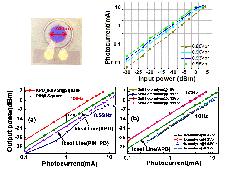
Dual M-Layers Avalanche Photodiodes with High Single-Photon Detection Efficiency and High Saturation Output Power for Lidar applications
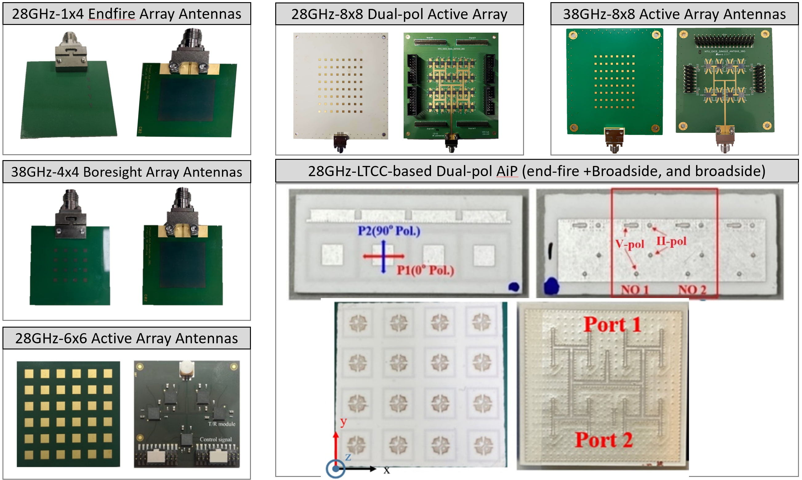
Antenna-in-package (AiP) Technology Suitable for Feeding to the Smart Impedance Material for High-Gain Radiations at Millimeter Wave Frequencies
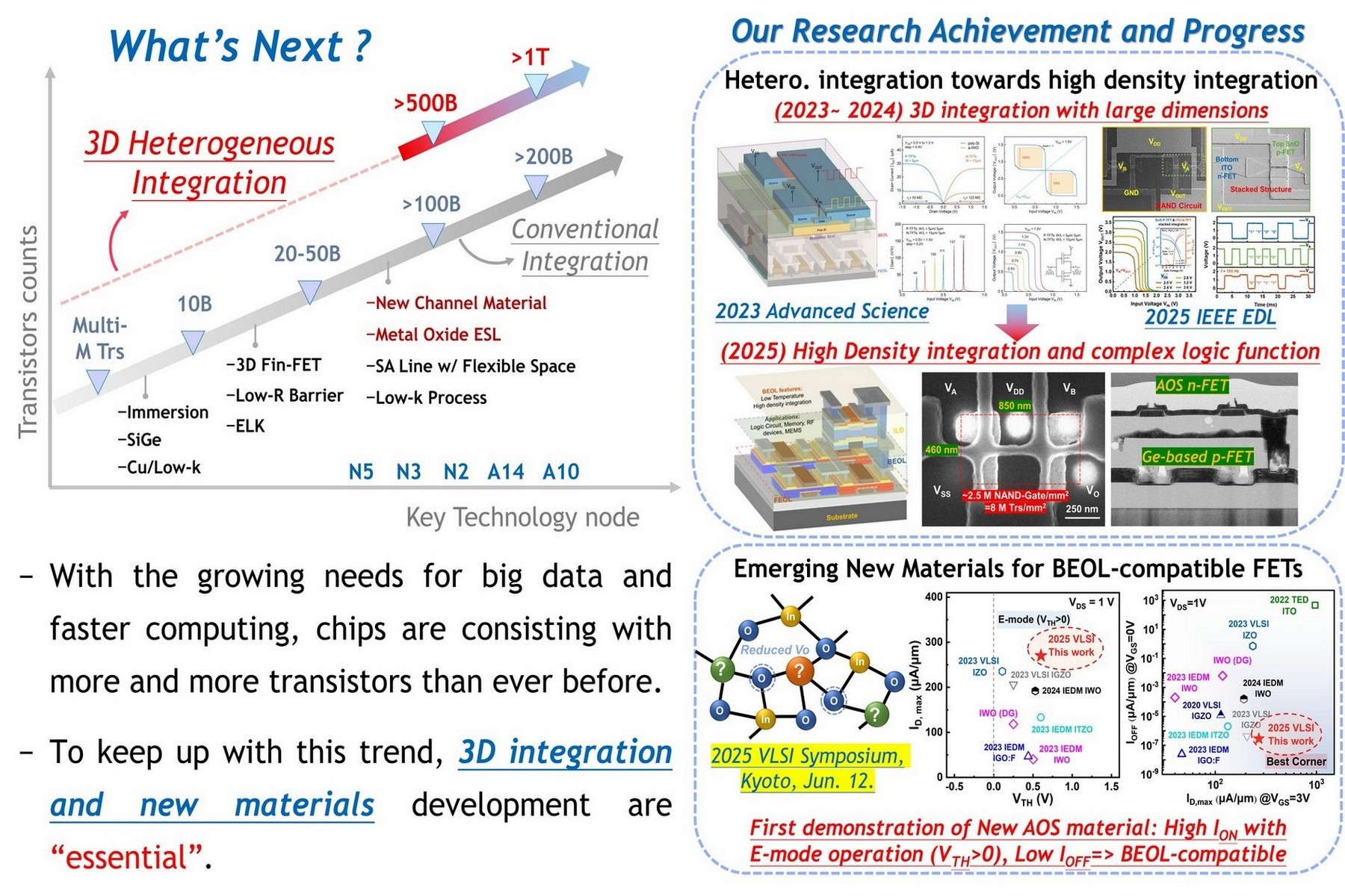
Monolithic 3D Heterogeneous Device Integration and Innovative Materials for Breaking Logic Density Limits: A Key Technology Platform for High-Density AI Computing Chips
Technology maturity:Mass production
Exhibiting purpose:Product promotion、Display of scientific results
Trading preferences:Technical license/cooperation
*Organization
*Name
*Phone
*Main Purpose
*Discuss Further
*Job Category
*Overall Rating
*Favorite Area
*Key Tech Focus
*Willing to Receive Updates?
Other Suggestions
Coming soon!