Monolithic 3D Heterogeneous Device Integration and Innovative Materials for Breaking Logic Density Limits: A Key Technology Platform for High-Density AI Computing Chips
Technology Introduction:
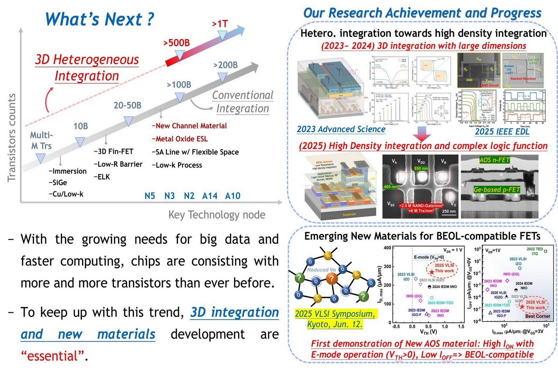
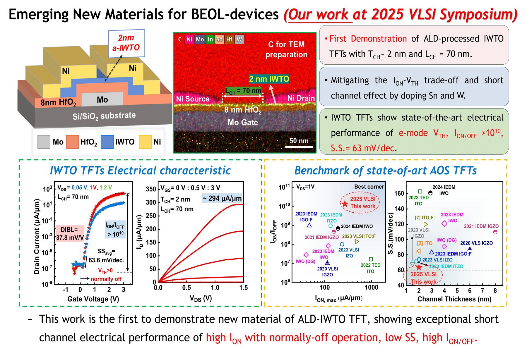
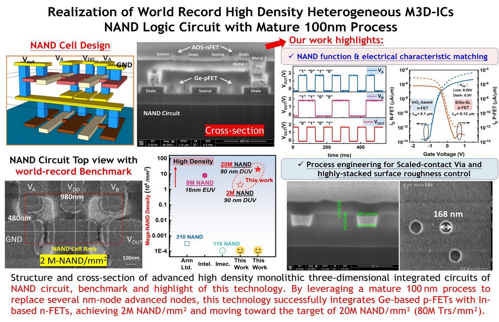
By leveraging a mature 100 nm process to replace sub-16 nm advanced nodes, this technology successfully integrates Ge-based p-FETs with In-based n-FETs featuring nanoscale channel thickness, achieving 2M NAND/mm² and moving toward the target of 20M NAND/mm² (80M Trs/mm²). In addition, this team pioneered a high-performance InWSnO transistor with an ultra-high on/off ratio and low subthreshold swing (SS), demonstrating strong potential for AI and HPC chip applications.
Industry Applicability:
This proposed 3D-IC achieves a world-leading transistor density and enabling logic circuits up to 8M Trs/mm² with a mature 100 nm-node process, instead of advanced several nm-node one. The core technology has been granted a Taiwan patent and a U.S. patent, demonstrating high commercialization potential. This work also pioneered the InWSnO TFT development, featuring excellent electrical performance, forming a key foundation for advancing next-generation 3D-IC technology.
National Yang Ming Chiao Tung University (NYCU) was formed in 2021 through the merger of National Yang Ming University and National Chiao Tung University. Located in Hsinchu, Taiwan, NYCU is a leading institution specializing in technology, engineering, medicine, and social sciences. The university is known for its strengths in research and innovation, particularly in areas such as information technology, biomedicine, and artificial intelligence. NYCU fosters interdisciplinary collaboration, global partnerships, and aims to nurture professionals with strong academic foundations and leadership skills to address societal challenges and contribute to technological advancements.
Name:Po-Tsun Liu
Phone:03-571-2121 #52994
Address:No. 75, Boai Street, Hsinchu 300, Taiwan, ROC
TWI805116B
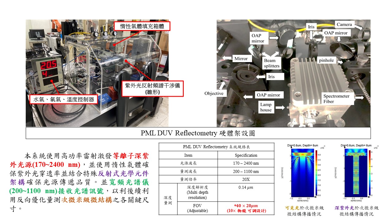
Optical critical-dimension measuring technology for high-aspect-ratio microstructures in advanced semiconductor packaging
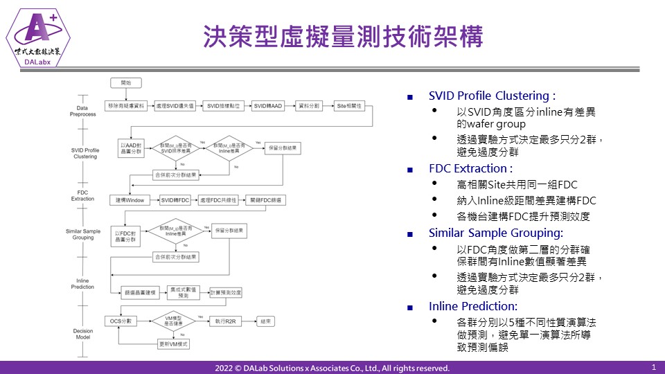
Optimizing Advanced Process Control Decision and Virtual Metrology Technology for Nano Technology Nodes for Semiconductor Manufacturing
6G FR3 RF front-end chipMassive MIMO four-port integrated antenna array technology6G FR3 RF front end module
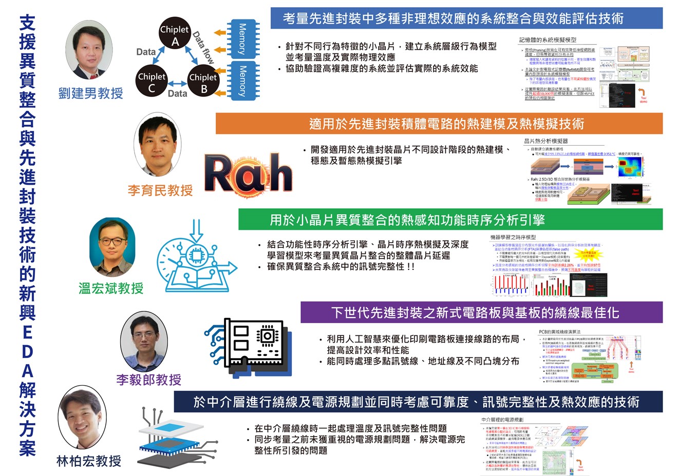
EDA solutions for Heterogeneous Integration and Advanced Packaging Technologies
Technology maturity:Others
Exhibiting purpose:Display of scientific results
Trading preferences:Negotiate by self
*Organization
*Name
*Phone
*Main Purpose
*Discuss Further
*Job Category
*Overall Rating
*Favorite Area
*Key Tech Focus
*Willing to Receive Updates?
Other Suggestions
Coming soon!