Optical critical-dimension measuring technology for high-aspect-ratio microstructures in advanced semiconductor packaging
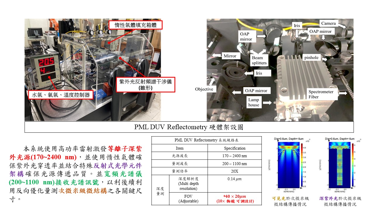
Severe technical challenges and bottlenecks to quality monitoring, especially in critical dimensional measurement for vias below 1 micrometer are currently faced in advanced packaging. To break through the bottleneck, broadband deep-ultraviolet light (DUV) is proposed to develop a novel optical system, so the optical wave can penetrate through the test structure effectively. More importantly, the proposed optical approach based on reflectometry and scatterometry is integrated with novel AI machine-learning optimization to achieve the best multi-CD measurement. As proved by industrial via tests, the method is capable of measuring CDs of submicron vias and RDL, which is regarded as the best measuring specification in the world.
The innovative technology that turns waste into treasure – Silicon Dioxide regenerated from semiconductor waste that contains Silicon
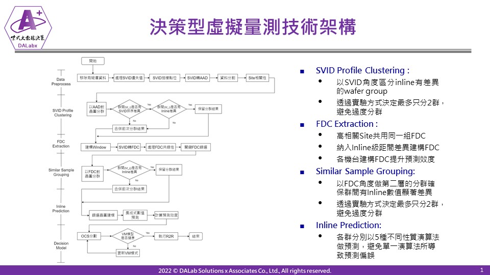
Optimizing Advanced Process Control Decision and Virtual Metrology Technology for Nano Technology Nodes for Semiconductor Manufacturing
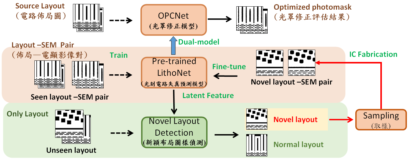
Deep learning-based EDA tools for lithography simulation, photomask correction, and novel layout patterns detection
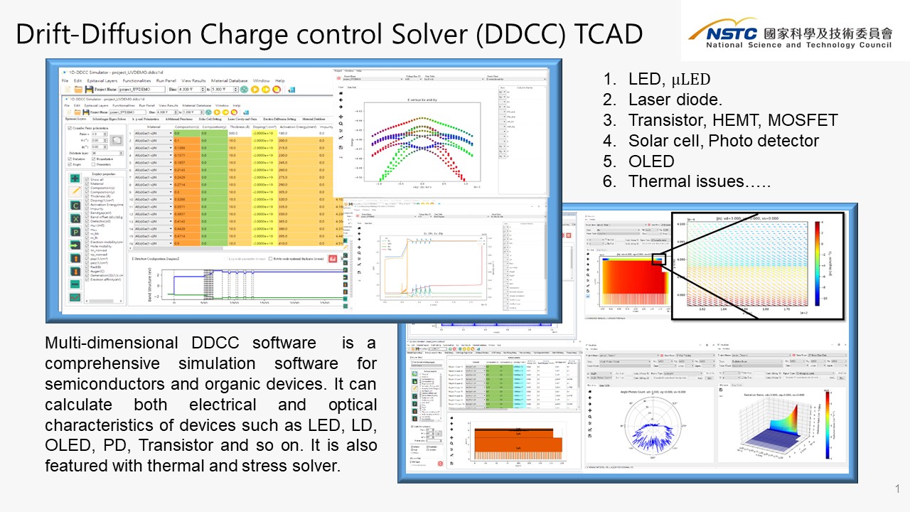
A Multi-Physics Coupled Simulation Platform for Next-Generation Wide-Bandgap Semiconductors (DDCC-TCAD)
Technology maturity:Prototype
Exhibiting purpose:Display of scientific results
Trading preferences:Exclusive license/assignment、Technical license/cooperation、Negotiate by self
*Organization
*Name
*Phone
*Main Purpose
*Discuss Further
*Job Category
*Overall Rating
*Favorite Area
*Key Tech Focus
*Willing to Receive Updates?
Other Suggestions
Coming soon!