Deep learning-based EDA tools for lithography simulation, photomask correction, and novel layout patterns detection
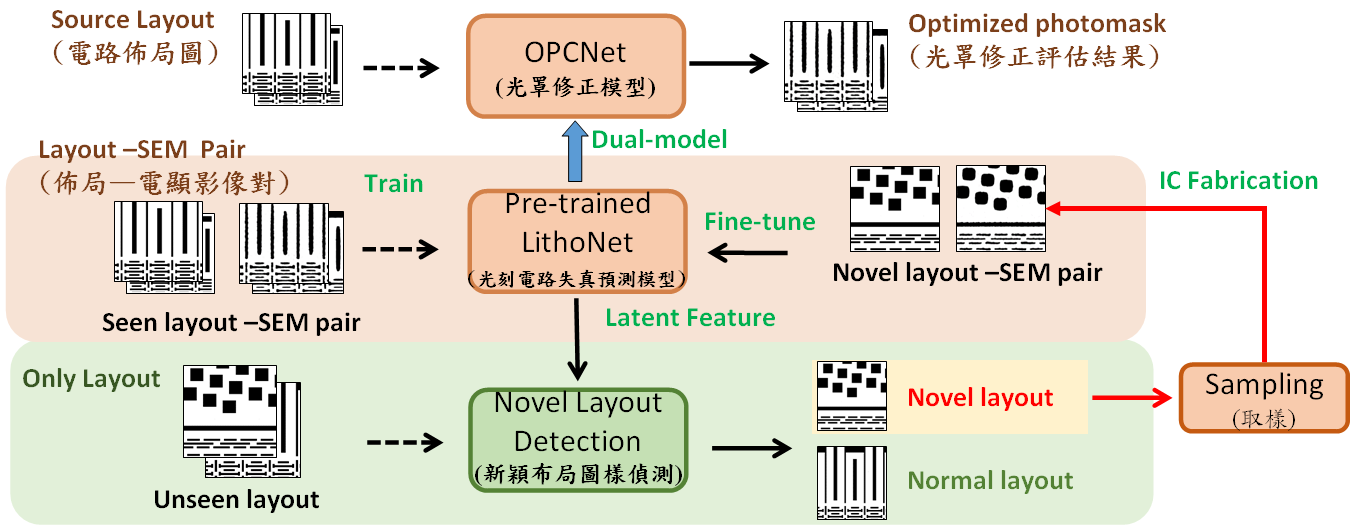

The DNN models of this technology include a LithoNet, an OPCNet, and a layout novelty detection network. LithoNet is a learning-based pre-simulation model for layout-to-SEM contour prediction, and OPCnet is a dual network of LithoNet for photomask optimization. Integrated with a well-trained LithoNet, our layout novelty detection network, consisting of a self-attention guided LithoNet and an autoencoder, can check if there are layout patterns easily resulting in local distortions in contours of metal lines based on multi-modal (global-local) feature fusion.
This is the first set of image-based layout-to-SEM prediction, photomask optimization, and layout novelty detection methods. Given different training ADI/AEI images, this technology can learn the knowledge of photolithograph and etching effects. It can thus help semiconductor manufacturers to predict the shape of metal layers of IC products and detect layout novelties. Also, this learning-based technology can be easily extended by collecting suitable layout-SEM image pairs of different fabrication configurations. Hence, it sets a new milestone and breakthrough for EDA tool development.
Compared with existing commercial rule-based software designed for analyzing ADI (after-development-image), the proposed technology comprising three learning-based methods can easily learn etching effects by training them on AEI (after-etching-image) image datasets. Therefore, this technology can also be used to predict layout-to-SEM contour deformations, optimized photo-masks, and layout novelty/weakness with respect to various fabrication parameters. Through this way, this technology can assist semiconductor manufacturers to save testing time and fabrication costs.
線上展網址:
https://tievirtual.twtm.com.tw/iframe/540e306e-a248-4f6b-8d65-7e5e1a1be1ab?group=23bfb1fa-dd5b-4836-81a1-4a1809b1bae5&lang=en
National Tsing Hua University (NTHU), established in 1911 and located in Hsinchu, Taiwan, is one of the top research universities in the country. NTHU offers a wide range of programs in fields such as engineering, science, management, and humanities. The university is known for its strong emphasis on innovation, research excellence, and fostering global perspectives. With a commitment to academic rigor and interdisciplinary collaboration, NTHU plays a key role in advancing knowledge and technological development, contributing to both Taiwan’s growth and the global academic community.
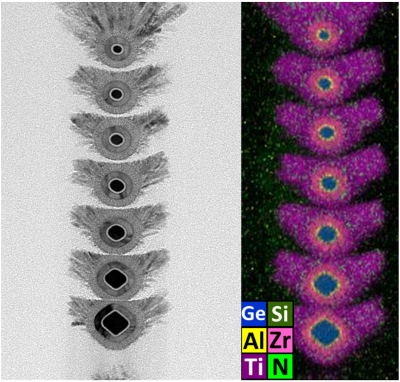
High mobility materials, process, stacked channels, and thermal circuit simulation; Ferroelectric X:HfO2 for Negative Capacitance and POC(Proof-of-Concept) Applications; Atomic layer technologies for
Transmitter and methods for frequency partitioning and parameter determing of cognitive frequency-hopping system
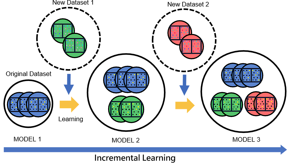
Sampling and Prediction of Photolithography Process and Applications of Incremental Learning Model
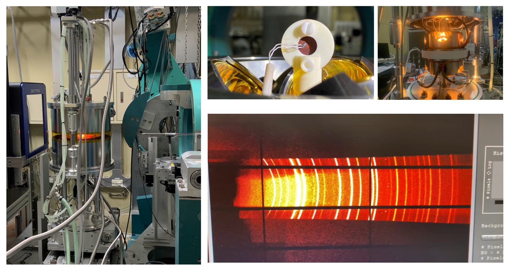
Refining area at 1600°C: Advanced synchrotron X-ray views into the black box of blast furnaces, understands ironmaking process, and illuminates the bright road to net-zero carbon emissions
Technology maturity:Experiment stage
Exhibiting purpose:Product promotion、Display of scientific results
Trading preferences:Technical license/cooperation、Negotiate by self
*Organization
*Name
*Phone
*Main Purpose
*Discuss Further
*Job Category
*Overall Rating
*Favorite Area
*Key Tech Focus
*Willing to Receive Updates?
Other Suggestions
Coming soon!