Dual M-Layers Avalanche Photodiodes with High Single-Photon Detection Efficiency and High Saturation Output Power for Lidar applications
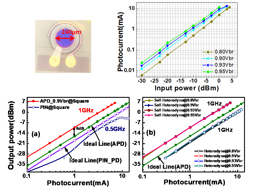

In this work, we demonstrate a dual multiplication layers In0.52Al0.48As based avalanche photodiode, which is desired for ToF lidar and FMCW lidar application due to its high performances in both Geiger and linear mode operations. By combining the specially designed mesa shape with dual M-layer structure, the edge breakdown can be well suppressed. We eventually achieve a single photon detection efficiency of 61.4% and neat temporal characteristic of 65ps without the involvement of afterpulsing at the gating frequency of 10 kHz for 200 K under Geiger mode operation. On the other hand, we can also achieve high gain-bandwidth product and high saturation current under linear mode (0.9 Vbr) operation. High photo-generated RF power from our APD with a high responsivity can be simultaneously achieved. The demonstrated APD opens new possibilities in the receiver-end of next generation lidar.
We achieve a single photon detection efficiency of 61.4% and neat temporal characteristic of 65ps without the involvement of afterpulsing at the gating frequency of 10 kHz for 200 K in Geiger mode operation. On the other hand, we can also achieve high gain-bandwidth product (450GHz) and high saturation current (>12mA) under linear mode operation. The corresponding photo-generated RF power from our APD can be as high as +6.95 dBm at a high (7 mA) output photocurrent. The demonstrated APD opens new possibilities in the receiver-end of next generation lidar.
LiDAR has become a crucial technology in many different areas including robots, scientific research, remote sensing and medical applications as well as in autonomous vehicle there has been tremendous progress attained over the past few years. The two most used lidar techniques which meet these requirements, involve the pulsed beam (based on the time of flight (ToF) principle) and frequency-modulated continuous wave (FMCW) approaches.
The detector technology we demonstrate here can further improve the sensitivity in such two kinds of lidar systems.
線上展網址:
https://tievirtual.twtm.com.tw/iframe/fb3becba-9752-4ea7-8652-38b43a70bfa4?group=23bfb1fa-dd5b-4836-81a1-4a1809b1bae5&lang=en
National Central University is a public research university with long-standing traditions of the Republic of China based in Taiwan. It was founded in 1902 and renamed in 1915. The school was initially located in Miaoli when it first moved to Taiwan, but relocated to Zhongli in 1962 and developed into a comprehensive university. It's the first university in Taiwan to research industrial economics,[3] and economic development (Taiwan's Consumer Confidence Index is released monthly by NCU).[4] NCU is a member of AACSB.[5] NCU is one of the six national universities in research selected by the Ministry of Education.
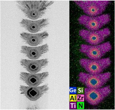
High mobility materials, process, stacked channels, and thermal circuit simulation; Ferroelectric X:HfO2 for Negative Capacitance and POC(Proof-of-Concept) Applications; Atomic layer technologies for
Hybrid CMOS Inverter Comprised of Thin Film Transistors with Hetero-channel for Monolithic 3D-ICs and Ultra-high Resolution Flat-Panel Displays Applications
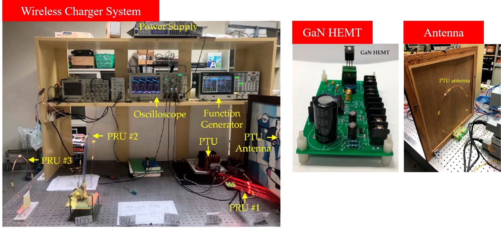
The novel technology of high efficiency GaN transistors for high frequency and high power application.
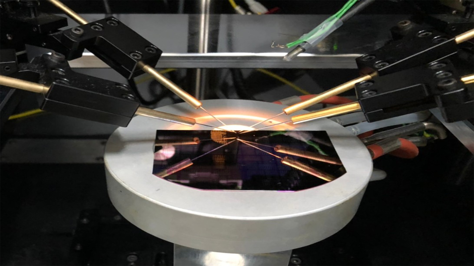
Low Temperature Polycrystalline Silicon Oxide (LTPO) TFT Architecture with Memory-embedded in Pixel for High-resolution and Power-saving Near-eye VR/AR Displays Applications
Technology maturity:Experiment stage
Exhibiting purpose:Product promotion、Display of scientific results
Trading preferences:Exclusive license/assignment、Negotiate by self
*Organization
*Name
*Phone
*Main Purpose
*Discuss Further
*Job Category
*Overall Rating
*Favorite Area
*Key Tech Focus
*Willing to Receive Updates?
Other Suggestions
Coming soon!