High mobility materials, process, stacked channels, and thermal circuit simulation; Ferroelectric X:HfO2 for Negative Capacitance and POC(Proof-of-Concept) Applications; Atomic layer technologies for


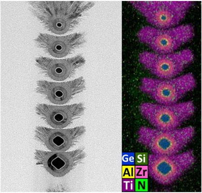
1.High mobility Ge channel stacked gate-all-around transistors
2.Fabrication of 3-D NCFETs, corresponding module development, ferroelectric tunneling memristor for neuromorphic computing, and the co-simulation between embedded memory and devices
3. Circuit level thermal-electrical SPICE modeling, providing the junction temperature and the temperature distribution in the metal lines for reliability prediction.

World-class ultra-precision optical processing technology and the non-contact floating display application
Hybrid CMOS Inverter Comprised of Thin Film Transistors with Hetero-channel for Monolithic 3D-ICs and Ultra-high Resolution Flat-Panel Displays Applications

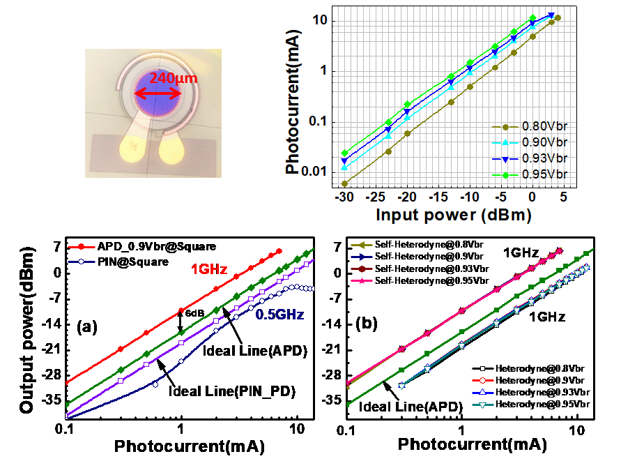
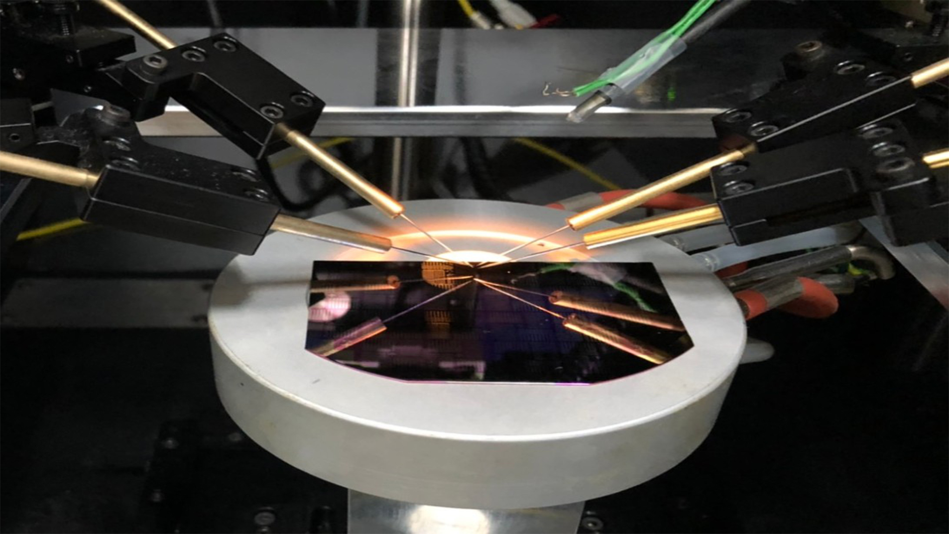
Dual M-Layers Avalanche Photodiodes with High Single-Photon Detection Efficiency and High Saturation Output Power for Lidar applications

Low Temperature Polycrystalline Silicon Oxide (LTPO) TFT Architecture with Memory-embedded in Pixel for High-resolution and Power-saving Near-eye VR/AR Displays Applications
Technology maturity:Experiment stage
Exhibiting purpose:Display of scientific results
Trading preferences:Technical license/cooperation
*Organization
*Name
*Phone
*Main Purpose
*Discuss Further
*Job Category
*Overall Rating
*Favorite Area
*Key Tech Focus
*Willing to Receive Updates?
Other Suggestions
Coming soon!