Hybrid CMOS Inverter Comprised of Thin Film Transistors with Hetero-channel for Monolithic 3D-ICs and Ultra-high Resolution Flat-Panel Displays Applications

AI and 5G technologies have emerged one after another, so that the size of transistor devices must continue to shrink according to Moore’s law to increase the speed and the performance of IC operations. As the device shrinks to the physical limit, the development of monolithic 3D-IC technology has received considerable attention.
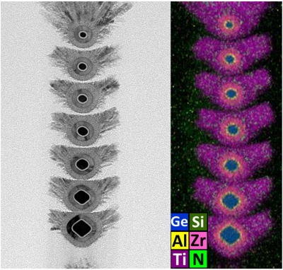
The objective of this project is to develop a novel HC-TFTs technology for the monolithic 3D-IC applications, which break through the technology bottlenecks of the traditional 2D-IC circuit architecture. With the HC-TFTs, the basic unit of logic circuits, inverter circuit, can be architected and process integrated in a single wafer further forming various functional circuits for achieving low-power consumption and high circuit integration.Through silicon via (TSV) technology has been adopted to achieve multi-chip modules with different IC functions for applications in the 3D-IC package architecture. However, the TSV technology suffers many challenges due to the limit in circuit layout and causing the decreased yield. Monolithic 3D-IC technology is expected to replace the TSV due to its ease of manufacture, short interconnections, lower power consumption, and lower cost. In this research, we have successfully developed the high-performance HC-TFTs comprised of N-channel a-IWO nano-sheet TFT and P-channel poly-Si TFT for monolithic 3D CMOS-based inverter applications. The technological breakthroughs are not only applied to 3D-IC, but can also be extended to ultra-high resolution flat-panel display backplane technology.This project has successfully developed a 3D-IC-based CMOS inverter circuit with high performance and low power consumption, which can be implemented in advanced electronic products. Also, the novel HC-TFT CMOS technology can be applied to flat-panel displays to construct the complete driving circuits and make the design of display circuits flexible, enhancing the diversity and added values.

High mobility materials, process, stacked channels, and thermal circuit simulation; Ferroelectric X:HfO2 for Negative Capacitance and POC(Proof-of-Concept) Applications; Atomic layer technologies for
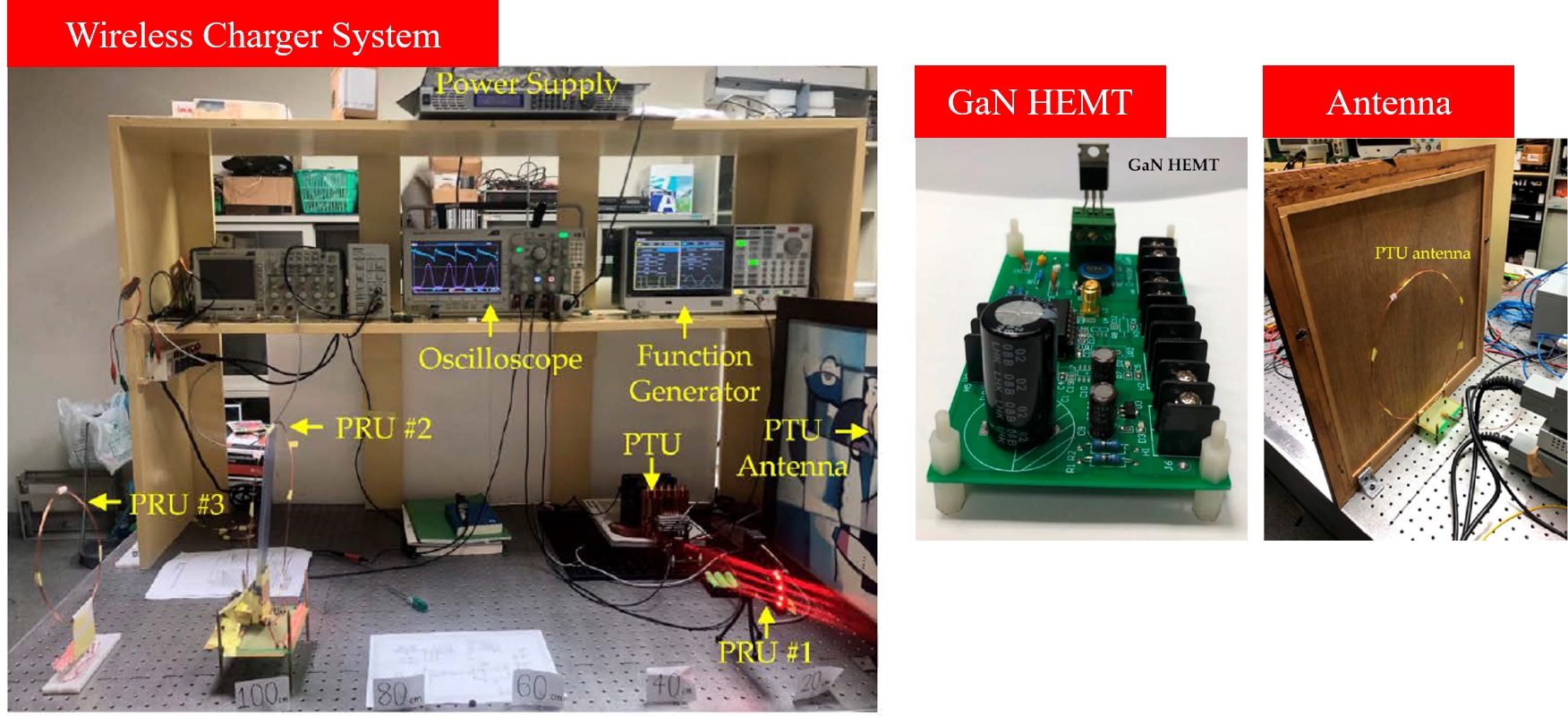
Resonant Magnetic Coupling Wireless Power Transfer System with Calibration Capabilities of Its Inductor-Capacitor Resonant Frequencies

The novel technology of high efficiency GaN transistors for high frequency and high power application.

Low Temperature Polycrystalline Silicon Oxide (LTPO) TFT Architecture with Memory-embedded in Pixel for High-resolution and Power-saving Near-eye VR/AR Displays Applications
Technology maturity:Experiment stage
Exhibiting purpose:Technology transactions、Product promotion、Display of scientific results
Trading preferences:Negotiate by self
*Organization
*Name
*Phone
*Main Purpose
*Discuss Further
*Job Category
*Overall Rating
*Favorite Area
*Key Tech Focus
*Willing to Receive Updates?
Other Suggestions
Coming soon!