Integrating Digital Grayscale, Defocus Method and Newly Developed Pho topolymer to Stereolithography 3D Printing Process to Rapidly Manufact ure Microlens Array with High Optical Performance


Microlens arrays (MLAs) have been widely applied. Currently, the fabricati
on of MLAs involves precise machining and photolithography, which suffe
r from high equipment costs, long production times and large amount of
wastes, and they also impose significant limitations on the shape of microl
enses. Digital light processing (DLP) 3D printing technology offers advant
ages such as low cost, shorter production time and being more environme
ntally friendly. However, the surface roughness of MLAs produced by DLP
3D printing technology is difficult to meet the requirements of optical co
mponents due to stair effect.
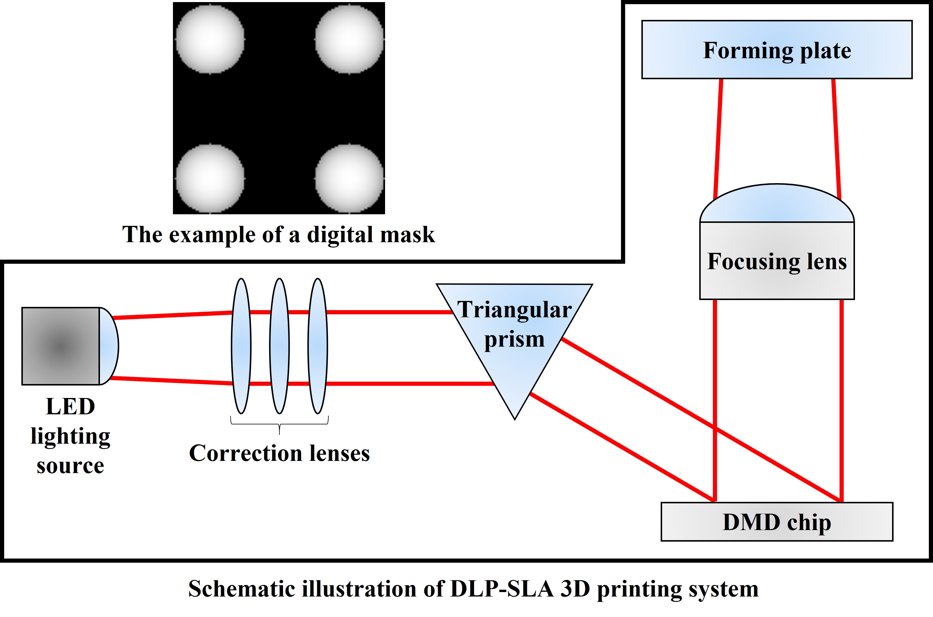
Our team employed adjustable grayscale masks in the manufacturing pro
cess. By adjusting the imaging position of the digital mask and the distanc
e between the mask and the forming platform, we create a defocus metho
d to eliminate stair effect and enabling the surface roughness of the micro
lens array to meet the requirements of optical components. Compared to
traditional processes, our technology can achieve MLA shapes that were p
reviously unattainable. In addition to the aforementioned manufacturing
method, our team has also utilized newly developed photopolymer specifi
cally designed for optical components. The goal is to enhance the resoluti
on, numerical aperture, and size limits of the micro lens array, thereby gre
atly expanding its range of applications.
It takes 1 second to solidify the polymer, and the entire fabrication proces
s takes 15 minutes. The resulting surface roughness is below 50 nm, while
the lens resolution can reach 58.7 lp/mm, which is more than that of com
mercial MLAs (resolution ~ 55 lp/mm). The diameter of the microlens is as
small as 60 μm. It is possible for us to fabricate microlens with high numer
ical apertures (0.98), multiple focal lengths (20 μm to 200 μm), and high fil
l factor (77.98%). The MLAs in this study can be applied to image panels a
nd sensors, and their optical performance are on par with commercial cou
nterp
Taiwan Tech has five campuses: the main Taipei campus and branch campuses at Tu-Cheng, Keelung, Gong-Guan, and Chupei, with a combined total area of 29.44 hectares. The main campus, situated in a district of Taipei with convenient transportation and beautiful surroundings, covers an area of about 10 hectares. Current enrollment includes 5,605 undergraduates and 4,902 graduate students with 415 full-time faculties.

Green adsorption materials and energy-saving exhaust gas treatment equipment used in the treatment of industrial volatile organic compounds
Single-Stage Electronic Lighting Driver for LED Streetlight Applications with Features of High-Power-Factor and Soft-Switching
Integrated Method for Improving Production Rate of Biogas Using Lignocellu-losic Depolymerization with Anaerobic Digestion

The design development technology and Power Generation system of Organic Rankine Cycle and Trans-critical Organic Rankine Cycle for Conversion of Low-and-Medium Heat.
Technology maturity:Experiment stage
Exhibiting purpose:Display of scientific results
Trading preferences:Negotiate by self
Coming soon!