The Development of High-Quality 2D Semiconductors With In-Plane Anisotropy

We use "programmable vacuum tube sealing technology" and "chemical vapor transport method" to grow ReS2 and ReSe2 single crystals. Programmable vacuum tube sealing technology is a key issue for obtaining excellent quality of ReS2 and ReSe2 layered single crystals. We use a programmable graphic panel for controlling all the pneumatic valves of the vacuum system. When we evacuate or vent the quartz-sealing system, only the use of argon gas for passing through the valve and entering into the quartz tube. It is not necessary to vent the diffusion pump like the traditional way. Therefore, the speed for evacuation is fast and high vacuum of 2~3x10⁻⁶ Torr can be maintained for achieving high purity of the as-grown crystals. The sealing tube is completed by using acetylene and oxygen torch.Layered ReS2 and ReSe2 belong to TMDs that crystalized in distorted CdCl2 structure of triclinic symmetry. Unlike the other 2D TMDs as MoS2 and WSe2 are in-plane isotropic semiconductors, ReS2 and ReSe2 possess extra in-plane anisotropy on mechanical, electrical and optical properties of the materials. In the van der Waals plane, the highest conductivity is along b axis and the conductivity gradually decreased with the angle is increased. Thus, the field-effect transistors made by ReS2 and ReSe2 can choose different orientation to change the channel mobility. There are five band-edge excitons of different energy (namely E1ex, E2ex, E3ex, ES1ex and ES2ex) existed in our ReSe2 and ReS2 while only two excitons had been detected in other groups. It verifies high quality of our crystals.1.We can provide big layered single crystals of ReS2, ReSe2 and ReS2(1-x)Se2(x).
2.Offering technology transfer of vacuum and crystal-growth techniques.
3.Providing fabrication of prototype transistors and optoelectronic devices.
4.We can also offer services in characterization of 2D materials and devices.
Name:何清華
Phone:02-27303772
Address:No.43, Keelung Rd., Sec.4, Da’an Dist., Taipei 10607, Taiwan

Enhancing Anodization of Semiconductor Materials Technology with Waf er Bonding Transforming Interface Function

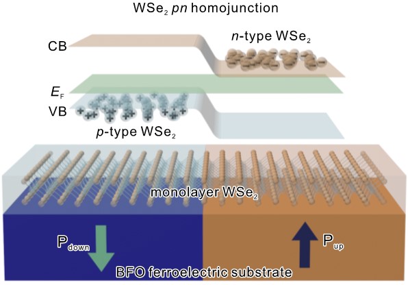
The realization of two-dimensional semiconductor device with atomic thickness

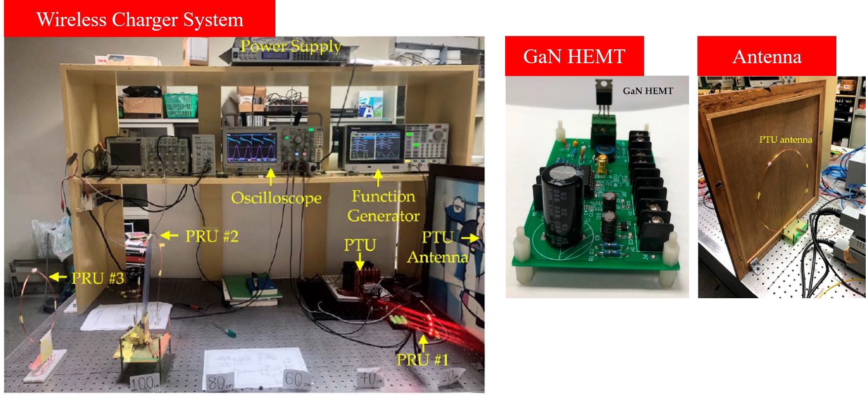
The novel technology of high efficiency GaN transistors for high frequency and high power application.

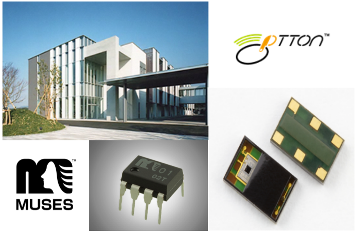
①The potential of Fukuoka Prefecture’s semiconductor industry ②High Quality Audio Device Series MUSES ③Optical Touchless Sensor"
Technology maturity:Trial production
Exhibiting purpose:Technology transactions、Product promotion、Display of scientific results
Trading preferences:Technical license/cooperation
Coming soon!