The realization of two-dimensional semiconductor device with atomic thickness
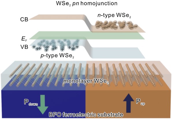
We proposed and showed the ferroelectric materials served as a prospective substrate to support TMD to achieve a pn homojunction, as the accumulation or depletion of an inevitably charged mobile carrier occurs in the TMD to screen the polarization field of the FE substrate. This work provides a non-volatile control of TMD doping and a promising way to produce a pn homojunction as a future building block of 2D device applications.
In recent years, the composite material made by combining materials have found ways to various applications including aviation, medicine, machinery, and construction. In this study, we used a 2D composite material composed of a single-layer WSe2 semiconductor and BiFeO3 to show that the electrical structure of the 2D material can be engineered without the addition of a metal electrode to achieve the effect of a diode. For the first time, it has been proved that the electronic structure of two-dimensional materials can be manipulated by the composite function of multiferroic materials.
We proposed and showed the ferroelectric materials served as a prospective substrate to support TMD to achieve a pn homojunction, as the accumulation or depletion of an inevitably charged mobile carrier occurs in the TMD to screen the polarization field of the FE substrate. This work provides a non-volatile control of TMD doping and a promising way to produce a pn homojunction as a future building block of 2D device applications.
線上展網址:
https://tievirtual.twtm.com.tw/iframe/ac63448e-9ffa-442d-93ff-5999a2b9454c?group=23bfb1fa-dd5b-4836-81a1-4a1809b1bae5&lang=en
NSRRC, the biggest large-scale shared research facility in Taiwan, currently operates two accelerators, the Taiwan Light Source (TLS) and the Taiwan Photon Source (TPS). TLS, of beam energy 1.5 GeV and circumference 120 meters, is the first third-generation synchrotron light source facility in Asia and the third globally. It has opened to users since October, 1993. The best optimized energy range of synchrotron light from TLS is between vacuum ultraviolet light and soft X-rays. The TPS, of circumference 518.4 meters, is one of the brightest synchrotron light sources in the world. It began its operation in September, 2016. To meet the demands from modern technologies and pioneer sciences for higher-brightness light beams, such as biomedicine and nanoscience, it is equipped with a low-emittance synchrotron storage ring and booster synchrotron producing a beam of energy 3 GeV. It generates X-rays in the higher energy range from soft X-rays to hard X-rays, and has a capacity of more than 40 beamlines. In addition, NSRRC built and operates two hard X-ray Taiwanese beamlines at SPring-8, Japan, as well as a cold neutron triple-axis spectrometer at the Australian Nuclear Science and Technology Organisation (ANSTO), under the international collaboration agreements. Scientists from around the world can access NSRRC’s facilities to explore the properties of materials in a wide range of disciplines through a competitive proposal process. Every year, over 2,000 users use NSRRC’s experimental facilities, which not only enable basic research, but also facilitate high-tech innovation. NSRRC possesses one of the most advanced synchrotron facilities in the world and its pioneering capabilities keep Taiwan at the forefront of scientific research.

Enhancing Anodization of Semiconductor Materials Technology with Waf er Bonding Transforming Interface Function
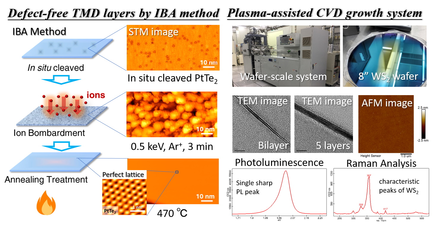
Beyond Silicon: Advanced Two-Dimensional Semiconductor Transistor Technologies
①The potential of Fukuoka Prefecture’s semiconductor industry ②High Quality Audio Device Series MUSES ③Optical Touchless Sensor"
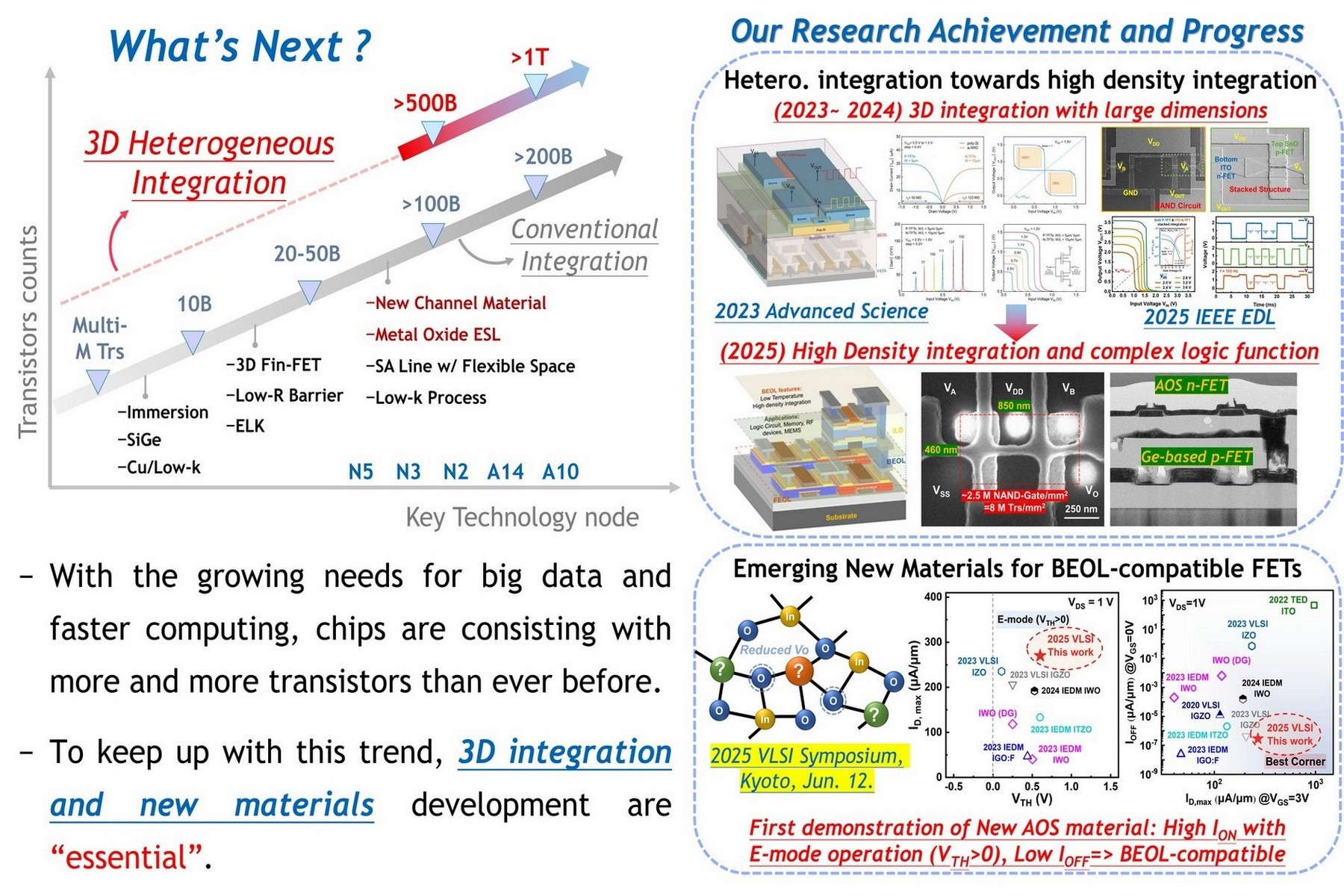
Monolithic 3D Heterogeneous Device Integration and Innovative Materials for Breaking Logic Density Limits: A Key Technology Platform for High-Density AI Computing Chips
Technology maturity:Experiment stage
Exhibiting purpose:Product promotion、Display of scientific results
Trading preferences:Technical license/cooperation
*Organization
*Name
*Phone
*Main Purpose
*Discuss Further
*Job Category
*Overall Rating
*Favorite Area
*Key Tech Focus
*Willing to Receive Updates?
Other Suggestions
Coming soon!