Beyond Silicon: Advanced Two-Dimensional Semiconductor Transistor Technologies
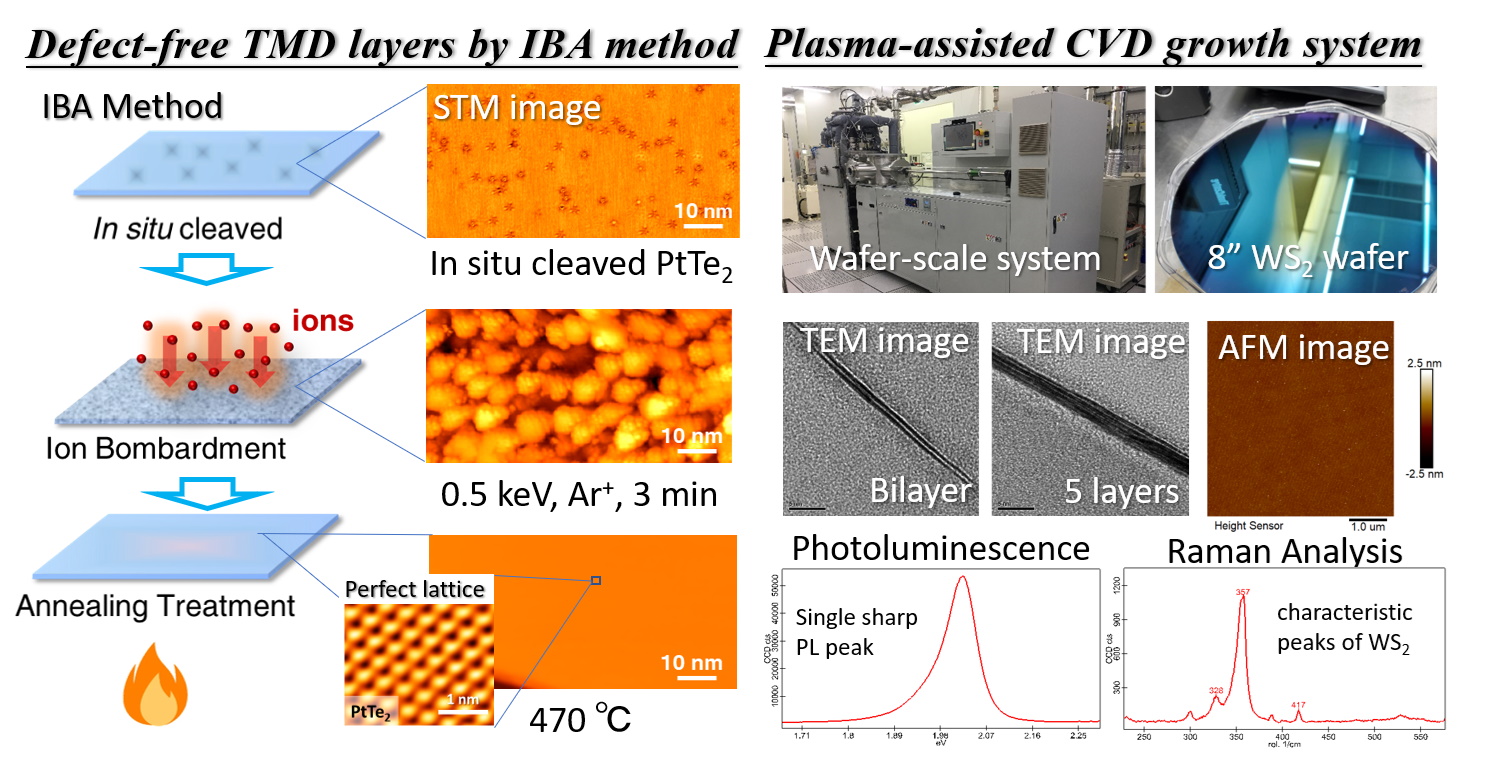
For the applications of two-dimensional (2D) semiconductors in future semiconductor technologies, several essential bottleneck problems are resolved. We develop an ion-bombardment and thermal annealing for repairing defects on surface of 2D semiconductors (such as PdTe2 and PtTe2), a high-speed switching of field-effect transistors (FETs) with ultrathin high-k Ta2O5 dielectrics, an extremely low-resistance contact technique with graphene and TaS2, low-temperature (250oC) epitaxy of h-AlN as dielectrics for gate-all-around field-effect transistors, and low-temperature (600oC) wafer-scale epitaxy of crystalline 2D semiconductors (WS2). These key advances push 2D semiconductors approaching feasible applications in future electronics.
National Yang Ming Chiao Tung University (NYCU) was formed in 2021 through the merger of National Yang Ming University and National Chiao Tung University. Located in Hsinchu, Taiwan, NYCU is a leading institution specializing in technology, engineering, medicine, and social sciences. The university is known for its strengths in research and innovation, particularly in areas such as information technology, biomedicine, and artificial intelligence. NYCU fosters interdisciplinary collaboration, global partnerships, and aims to nurture professionals with strong academic foundations and leadership skills to address societal challenges and contribute to technological advancements.
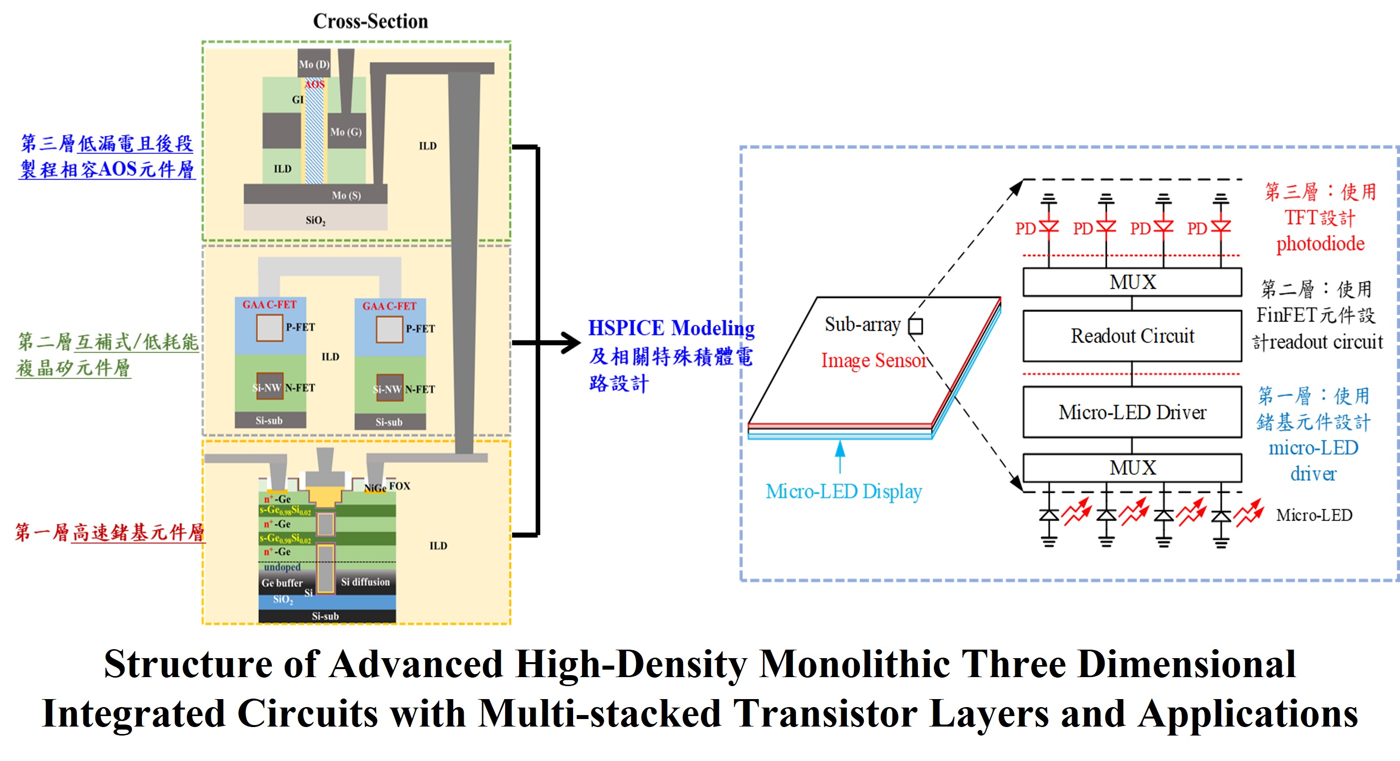
Development for Advanced High-Density Monolithic Three Dimensional Integrated Circuits with Multi-stacked Transistor Layers
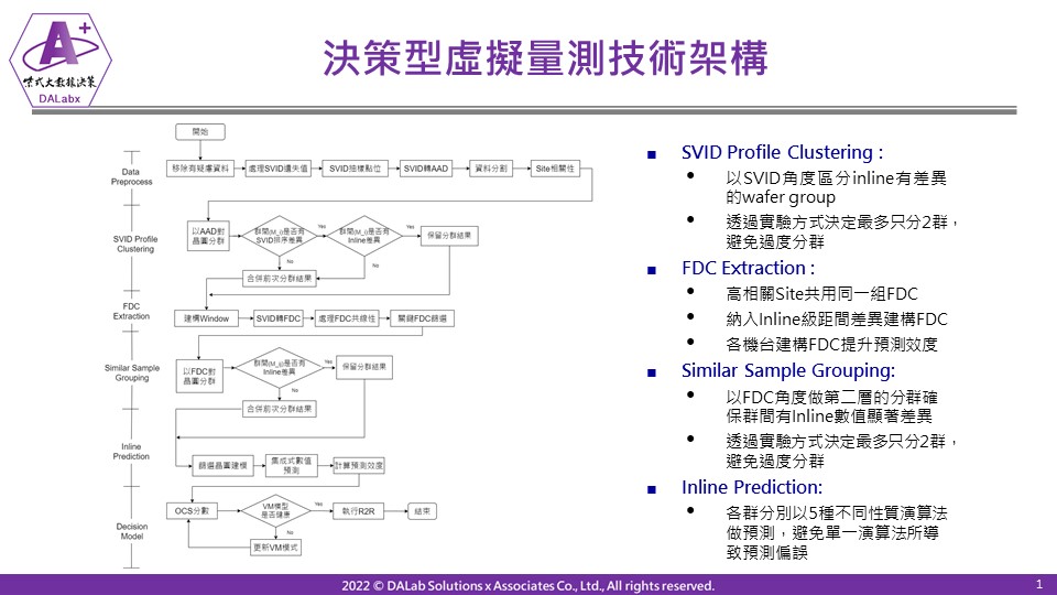
Optimizing Advanced Process Control Decision and Virtual Metrology Technology for Nano Technology Nodes for Semiconductor Manufacturing
High mobility materials, process, stacked channels, and thermal circuit simulation; Ferroelectric X:HfO2 for Negative Capacitance and POC(Proof-of-Concept) Applications; Atomic layer technologies for
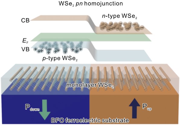
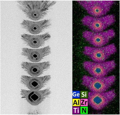
The realization of two-dimensional semiconductor device with atomic thickness
Technology maturity:Concept
Exhibiting purpose:Display of scientific results
Trading preferences:Exclusive license/assignment、Negotiate by self
*Organization
*Name
*Phone
*Main Purpose
*Discuss Further
*Job Category
*Overall Rating
*Favorite Area
*Key Tech Focus
*Willing to Receive Updates?
Other Suggestions
Coming soon!