Development for Advanced High-Density Monolithic Three Dimensional Integrated Circuits with Multi-stacked Transistor Layers
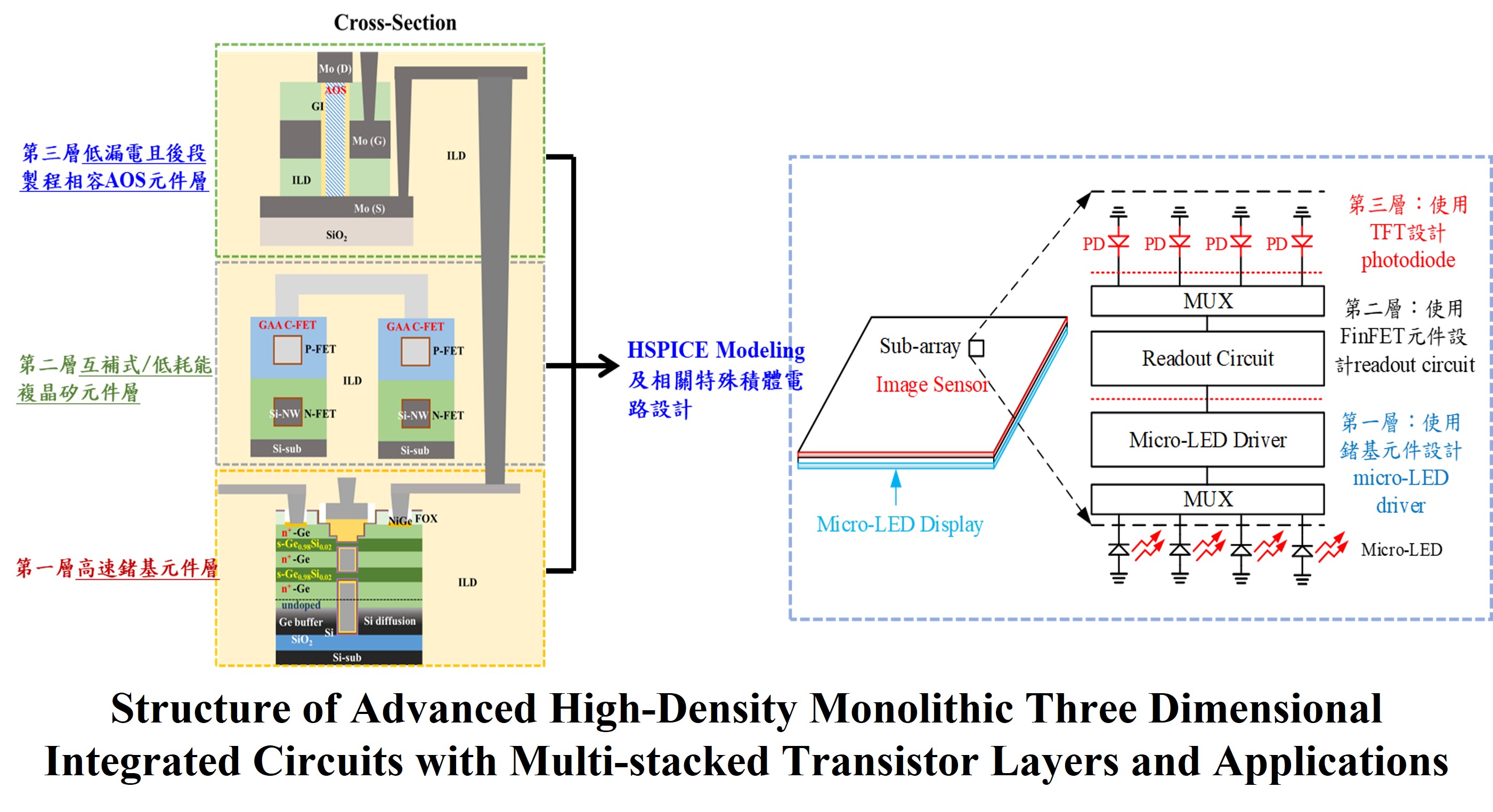
The aim of this project is to develop Advanced High-Density Monolithic Three Dimensional Integrated Circuits with Multi-stacked Transistor Layers by integrating three layers of high-performance stacked transistors and extending them to the circuit design of application-specific integrated circuits (ASICs). The research contents include the developments of novel semiconductor materials, high-performance GAAFET devices, the device model establishment, and circuit designs for ASICs. Based on the device models of three-layer stacked transistors, the driver IC design of augmented reality telescopes with image sensors and micro-LED display circuits is realized to demonstrate the technology feasibility of the proposed M3D-ICs.
National Yang Ming Chiao Tung University (NYCU) was formed in 2021 through the merger of National Yang Ming University and National Chiao Tung University. Located in Hsinchu, Taiwan, NYCU is a leading institution specializing in technology, engineering, medicine, and social sciences. The university is known for its strengths in research and innovation, particularly in areas such as information technology, biomedicine, and artificial intelligence. NYCU fosters interdisciplinary collaboration, global partnerships, and aims to nurture professionals with strong academic foundations and leadership skills to address societal challenges and contribute to technological advancements.
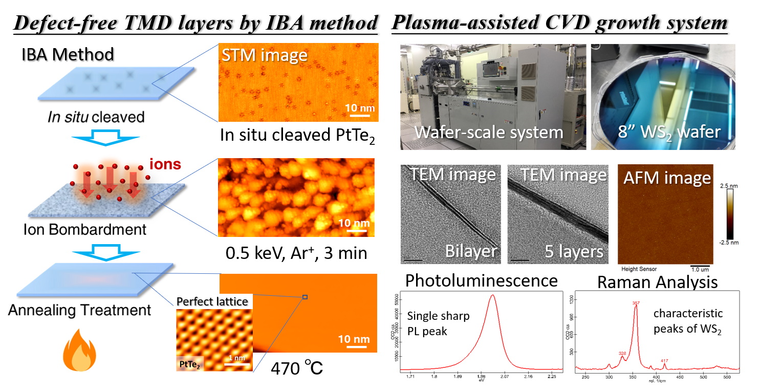
Beyond Silicon: Advanced Two-Dimensional Semiconductor Transistor Technologies
1.5-MHz High-Performance 380-V/12-V LLC Resonant Converters with Quarter-Turn Transformer Optimization
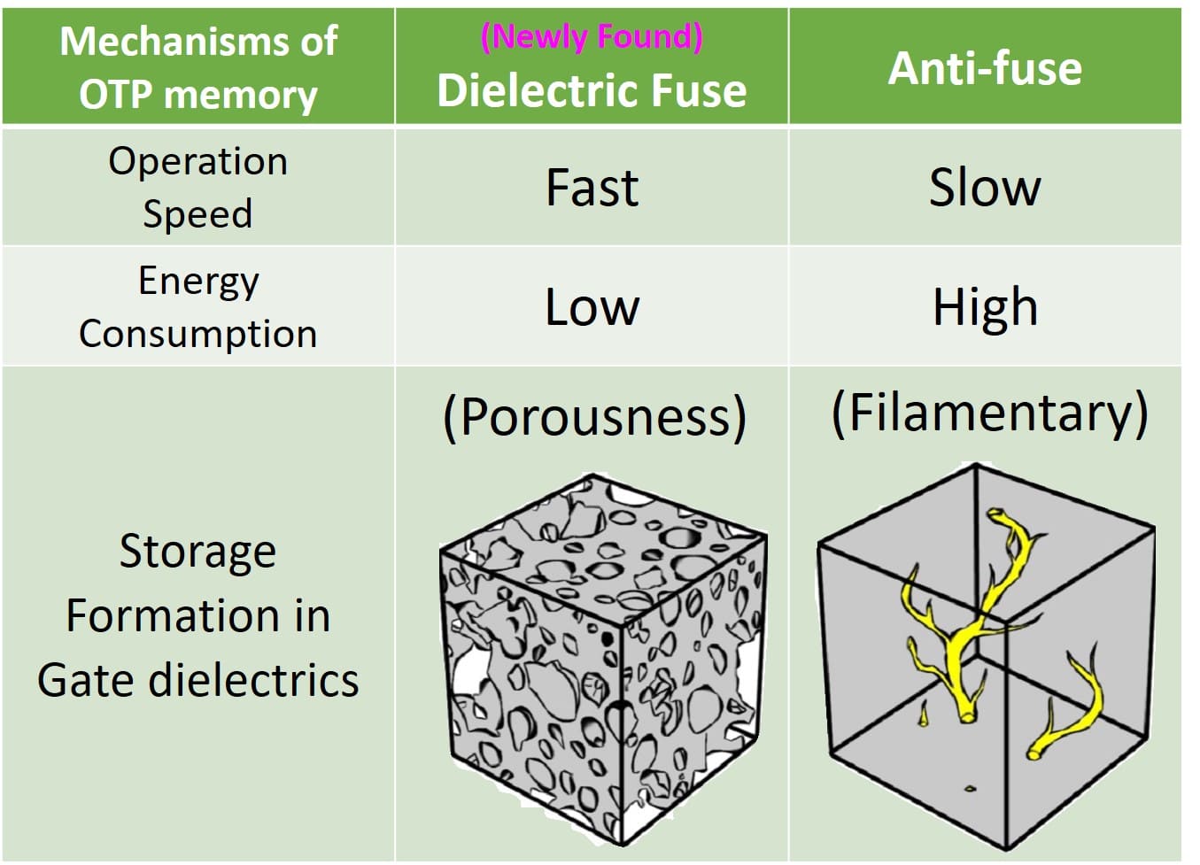
A Low-cost, Low-power, and High-speed “Dielectric-fuse Breakdown OTP” (dFuse OTP) Fully Integrated on CMOS Platform without Additional Masks
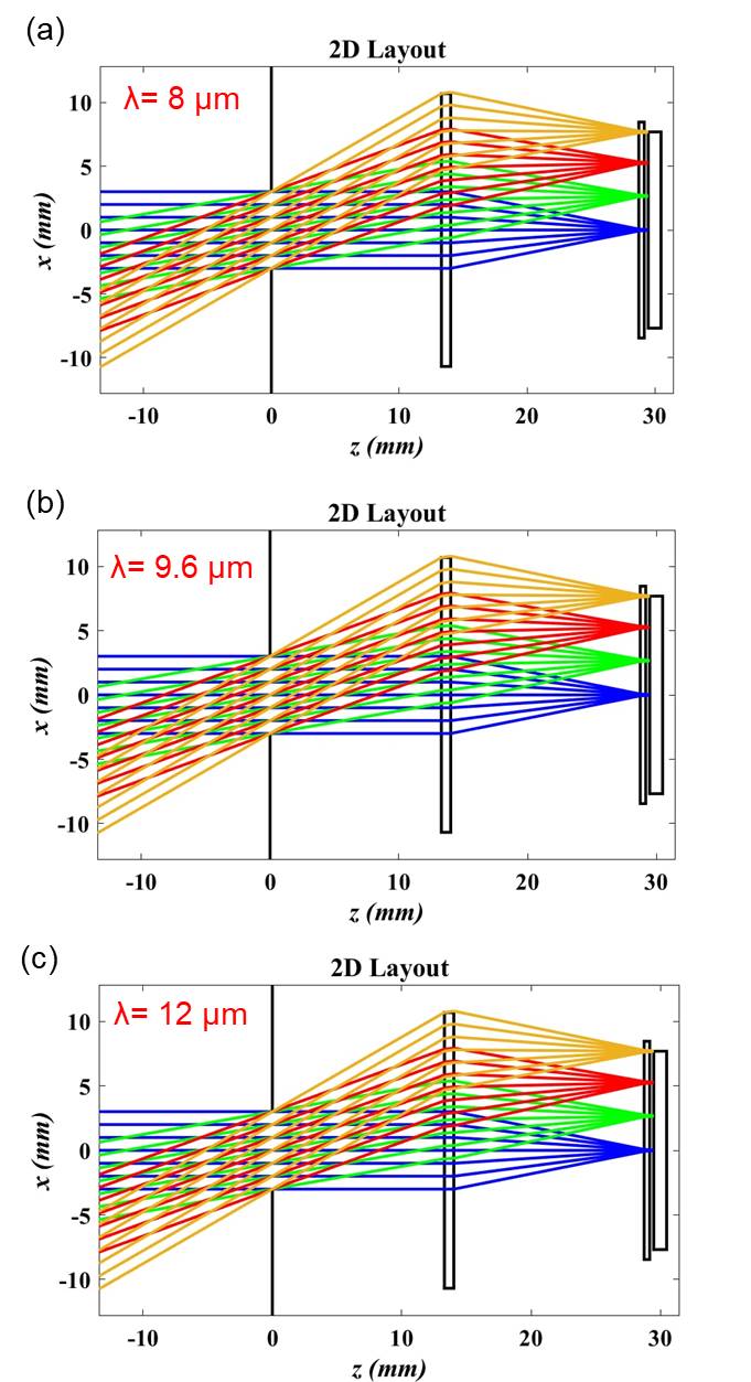
Self-Developed Monolithic Thermal Imaging Metalens with Achromatic and Aberration-Free Design
Technology maturity:Experiment stage
Exhibiting purpose:Display of scientific results
Trading preferences:Exclusive license/assignment、Technical license/cooperation、Negotiate by self
*Organization
*Name
*Phone
*Main Purpose
*Discuss Further
*Job Category
*Overall Rating
*Favorite Area
*Key Tech Focus
*Willing to Receive Updates?
Other Suggestions
Coming soon!