Self-Developed Monolithic Thermal Imaging Metalens with Achromatic and Aberration-Free Design
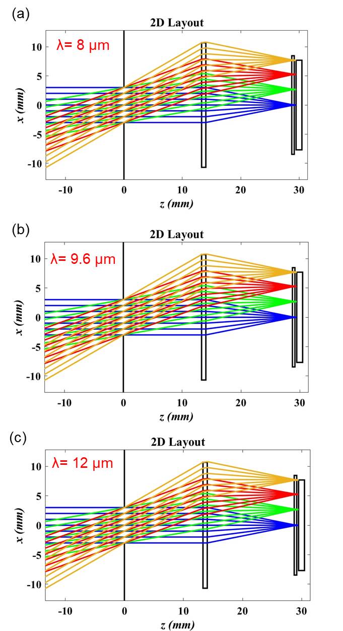

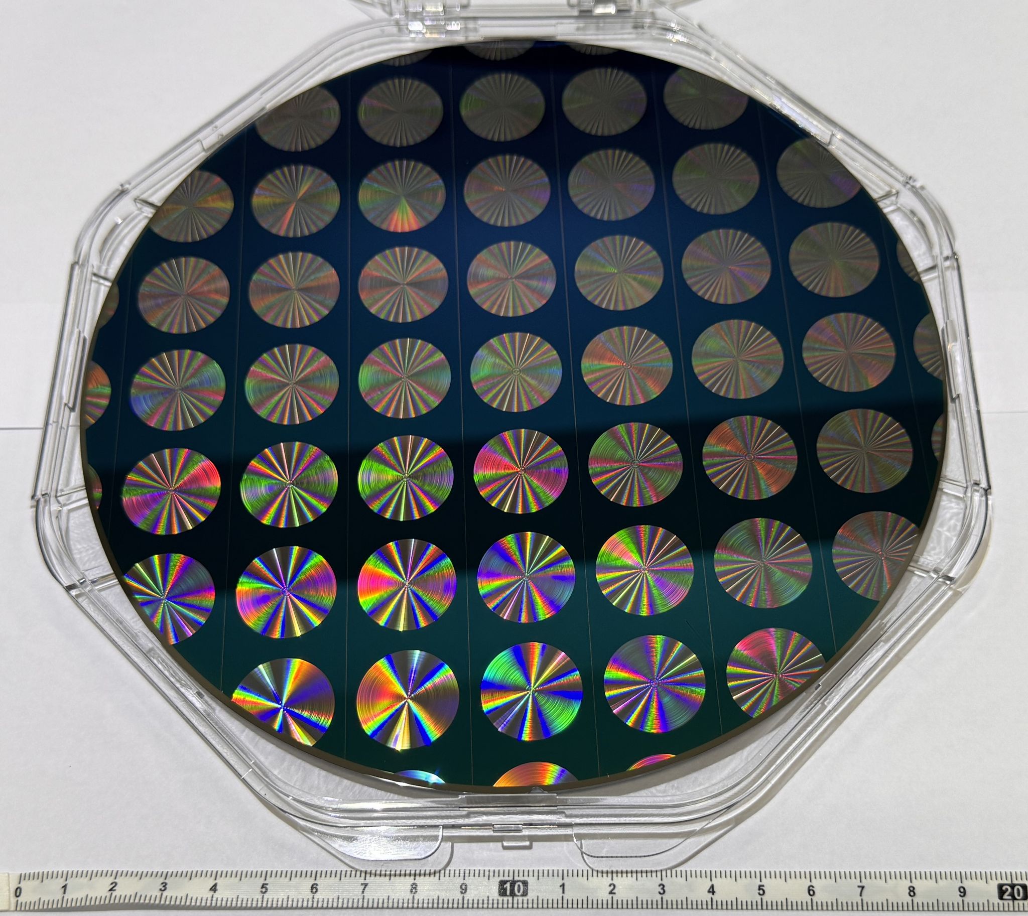


Using a self-developed optimization algorithm, we designed and fabricated Taiwan's first 2 cm thermal imaging metalens with a 60° field of view, aberration correction, and broadband achromatic performance (8-12 μm). This lightweight, 1-gram metalens is ideal for drones and aerospace, addressing reliance on imports and enhancing national security.
National Central University is a public research university with long-standing traditions of the Republic of China based in Taiwan. It was founded in 1902 and renamed in 1915. The school was initially located in Miaoli when it first moved to Taiwan, but relocated to Zhongli in 1962 and developed into a comprehensive university. It's the first university in Taiwan to research industrial economics,[3] and economic development (Taiwan's Consumer Confidence Index is released monthly by NCU).[4] NCU is a member of AACSB.[5] NCU is one of the six national universities in research selected by the Ministry of Education.
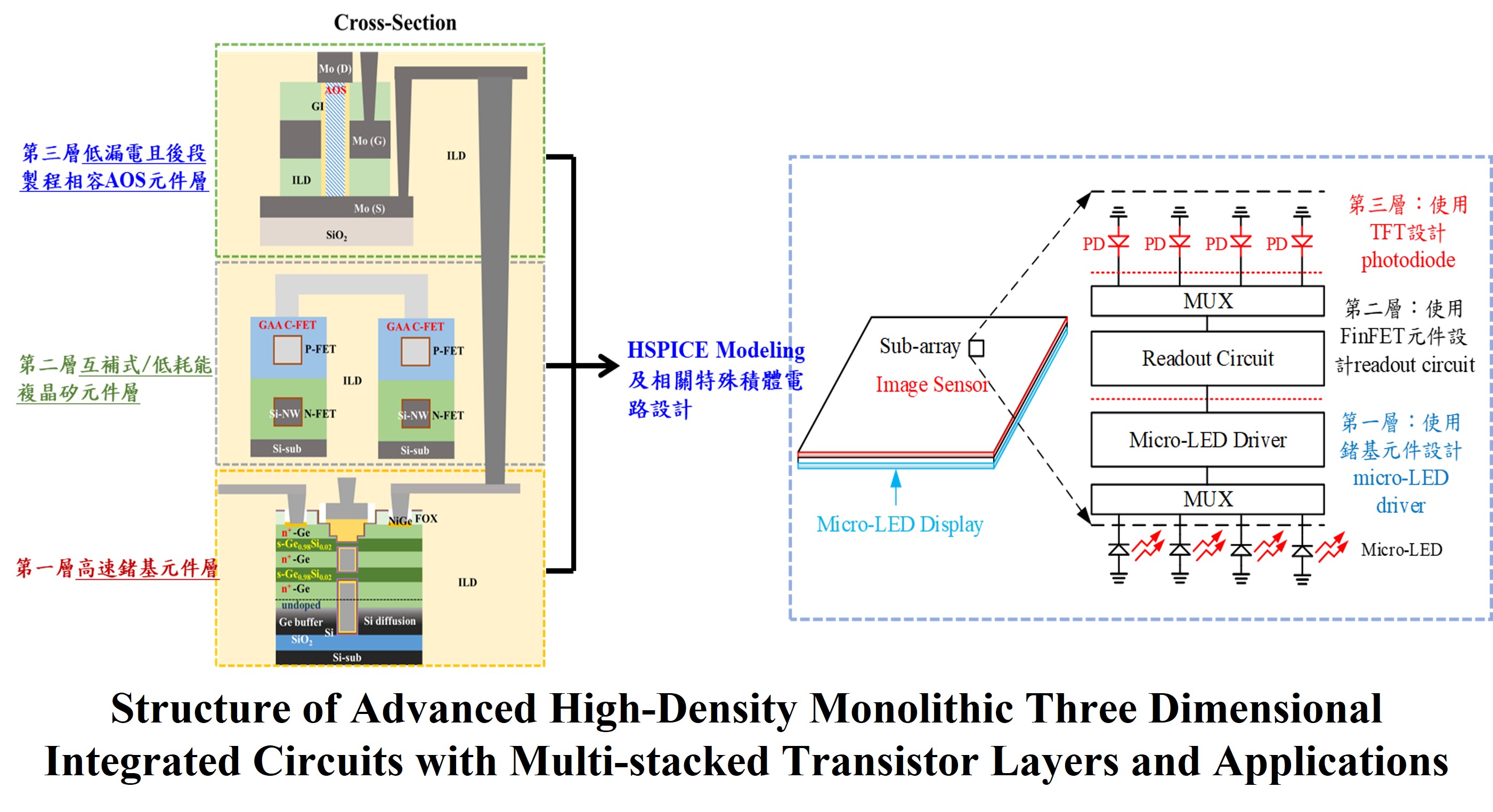
Development for Advanced High-Density Monolithic Three Dimensional Integrated Circuits with Multi-stacked Transistor Layers
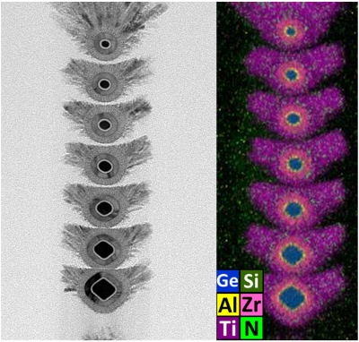
High mobility materials, process, stacked channels, and thermal circuit simulation; Ferroelectric X:HfO2 for Negative Capacitance and POC(Proof-of-Concept) Applications; Atomic layer technologies for
Towards Automatic Hyperspectral Imaging via the Combination of Sample Navigation MappingLaser Scanning Spectral Microscopy
Resonant Magnetic Coupling Wireless Power Transfer System with Calibration Capabilities of Its Inductor-Capacitor Resonant Frequencies
Technology maturity:Trial production
Exhibiting purpose:Display of scientific results
Trading preferences:Negotiate by self
*Organization
*Name
*Phone
*Main Purpose
*Discuss Further
*Job Category
*Overall Rating
*Favorite Area
*Key Tech Focus
*Willing to Receive Updates?
Other Suggestions
Coming soon!