Enhancing Anodization of Semiconductor Materials Technology with Waf er Bonding Transforming Interface Function

Electrochemical etching and the process of applying related principles are
important semiconductor material technologies, and are now also the key
technologies for fabricating nanostructures in nanotechnology. The key s
ubstance for the electrochemical etching chemical reaction is the hole (h
+), because the hole can enter the chemical bond connecting the solid sur
face atoms and weaken bond strength to result in etching.
Since the N-type silicon substrate lacks the element of anodic oxidation -
holes, this becomes the biggest obstacle in making the porous layer. The e
xisting method is to irradiate the surface or the back of the silicon substrat
e with strong light from a halogen lamp to generate holes to assist the etc
hing during etching. However, the hole density excited by projected light i
s easily affected by the intensity of the light source, distance, medium, wa
velength, etc., and is far less stable than anodic oxidation in a dark room.
This technology uses hydrophobic wafer bonding technology to bond P-t
ype silicon as an intermediary electrode on the back of N-type silicon to f
orm a detachable PN junction and then connect electrodes to form N-typ
e Si/P-type Si/ Electrode sandwich structure. The P-type silicon and N-typ
e silicon form a PN junction, which can convert the holes in the N-type sili
con from "secondary carrier flow" to "main control current", thus greatly i
mproving the anodic oxidation efficiency of the substrate surface . After t
he electrochemical etching process is completed, the P-type silicon used a
s the intermediary electrode can be easily separated from the N-type silic
on, so that the processed N-type silicon remains pure and free from pollut
ion. This technology has been successfully expanded from the application
of N-type silicon crystal materials to N-type silicon carbide materials. It is
expected to be extended and applied to other N-type semiconductor mat
erials.
National Central University is a public research university with long-standing traditions of the Republic of China based in Taiwan. It was founded in 1902 and renamed in 1915. The school was initially located in Miaoli when it first moved to Taiwan, but relocated to Zhongli in 1962 and developed into a comprehensive university. It's the first university in Taiwan to research industrial economics,[3] and economic development (Taiwan's Consumer Confidence Index is released monthly by NCU).[4] NCU is a member of AACSB.[5] NCU is one of the six national universities in research selected by the Ministry of Education.
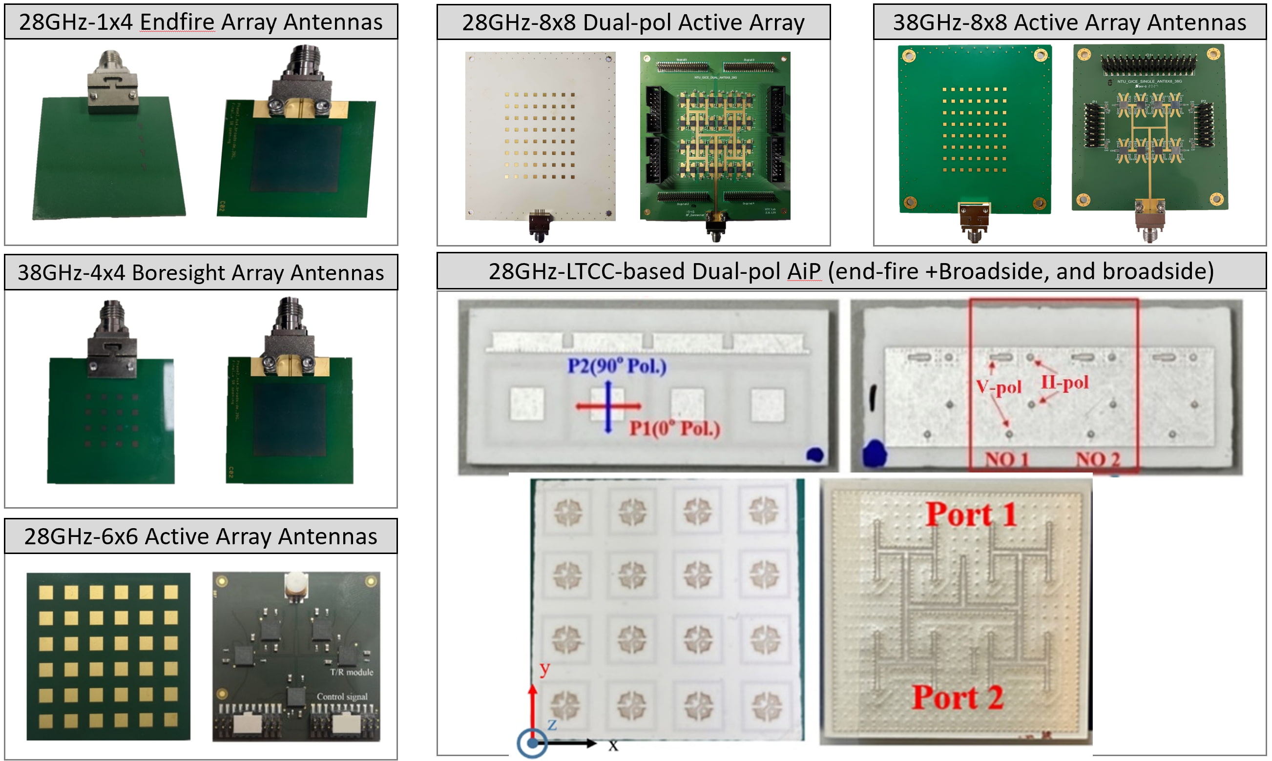
Antenna-in-package (AiP) Technology Suitable for Feeding to the Smart Impedance Material for High-Gain Radiations at Millimeter Wave Frequencies
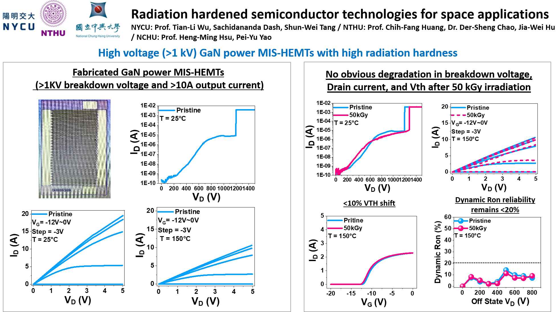
Radiation Hardened Semiconductor Technologies for Space Applications
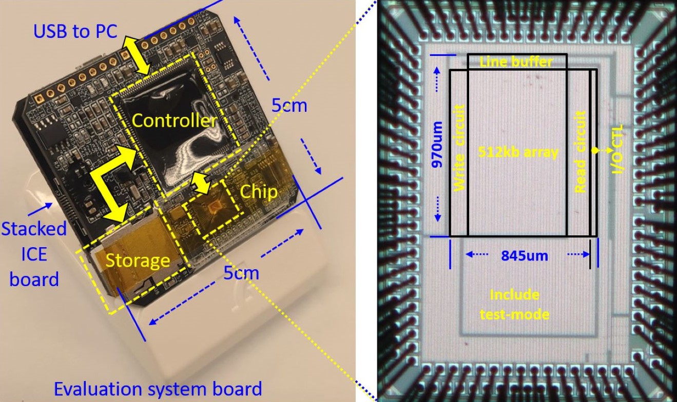
Energy-Efficient Optimization Problem Decision: Neural Network-based In-Memory Annealing Units for Route Scheduling and Genome Assembly
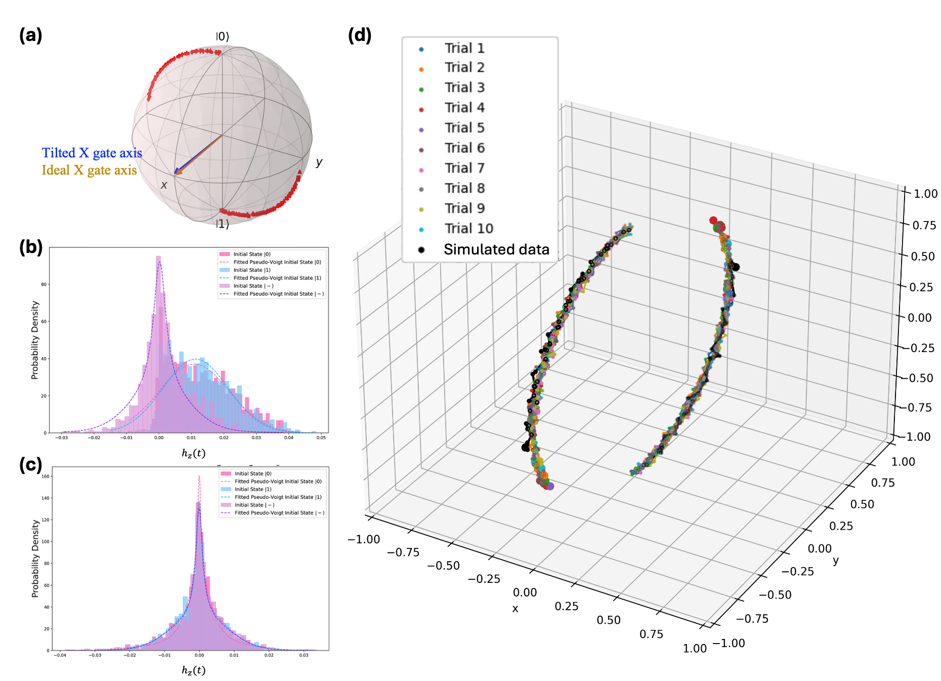
Exploring the Future of Chemistry and Materials Science through Quantum Noise Characterization and Simulation
Technology maturity:Experiment stage
Exhibiting purpose:Display of scientific results
Trading preferences:Negotiate by self
*Organization
*Name
*Phone
*Main Purpose
*Discuss Further
*Job Category
*Overall Rating
*Favorite Area
*Key Tech Focus
*Willing to Receive Updates?
Other Suggestions
Coming soon!