In-line semiconductor N2 process critical dimension X-ray metrology tool (XRCD)
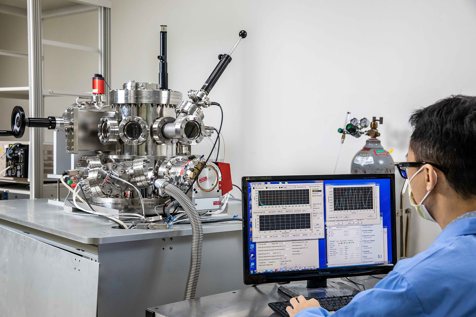
Semiconductor industry in Taiwan is in the R&D process of developing 2 nm technology node (N2) using Gate-All-Around (GAA) technology instead of Fin Field-Effect Transistor (FinFET) architecture used for 3 nm process. The world’s leading chipmaker in Taiwan expects to have pilot production starting in 2023 and high volume production later in 2024. As the GAA technology is introduced, not only is the feature size shrunk to 2 nm, but more complex and high precision 3D critical dimensions (CDs) with tighter tolerances are required to prevent the current leakage and increase the yield. As a result, significant metrology challenges are raised to maintain the high quality control of the front-end processes for the GAA transistors. Conventional metrology solutions, such as optical and SEM methods, are lack of sensitivity to monitor the complex 3D CDs of the GAA transistors in production with the demanded high precision. According to IRDS 2020, X-ray based methods have been identified as the only feasible in-line CD measurement solution for N2 GAA process. Therefore, the in-line X-ray critical dimention (XRCD) technology and an in-line measurement tool for α- site tests are established for the measurements of the complex 3D CDs of the GAA transistors. The XRCD is applied for in-die measurements with spot size of (50 50) µm2 and to provide accurate 3D CD measurements with an atomic-level resolution in the GAA front-end IC fabrication processes. With the successful establishment of the CD-XRR technology and the in-line measurement tool, it is expected to maintain competitiveness and strength the IC fabrication for the semiconductor industry in Taiwan. Additionally, the developed technology, then, will lead related domestic partners (equipment manufacturers) to become metrology tool suppliers in the front-end IC fabrication.
線上展網址:
https://tievirtual.twtm.com.tw/iframe/23dd0a9b-01f1-4146-a3d7-d4ba20cd78ef?group=f36efffd-9ee6-4962-aa09-72f6797d2449&lang=en
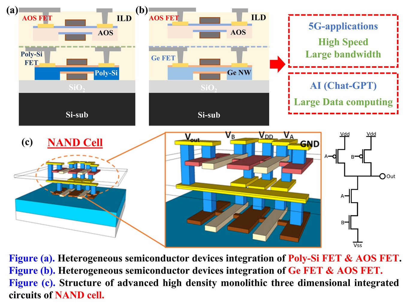
Novel Monolithic 3D Heterogeneous Semiconductor Device Integration f or Ultra-High-Density (20M NAND-Gate/mm^2) Logic Gate Circuits

Establishing dynamic models to evaluate the mode of transmission and e pidemic prevention measures for COVID-19.
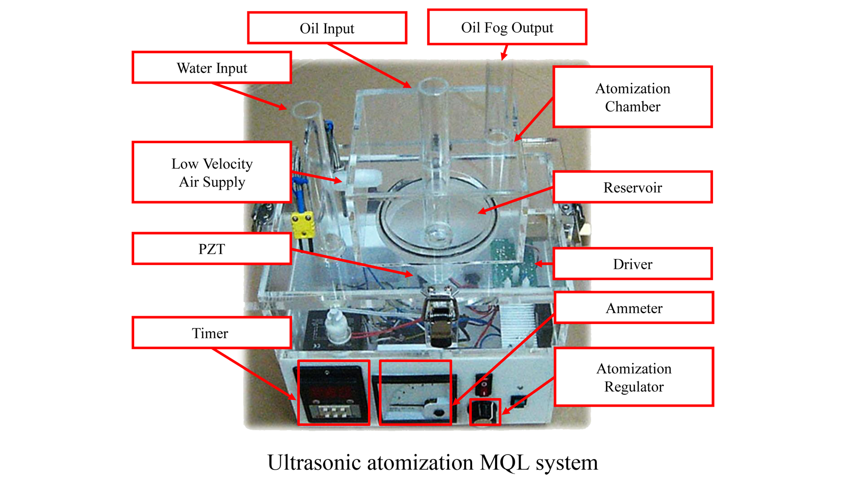
Nanofluid/ultrasonic atomization micro-lubrication system development and application intelligent modeling method to improve the multiple quality characteristics of the micro-machining process research and optimal prediction model establishment
①The potential of Fukuoka Prefecture’s semiconductor industry ②High Quality Audio Device Series MUSES ③Optical Touchless Sensor"
Technology maturity:Experiment stage
Exhibiting purpose:Technology transactions、Patent transactions、Product promotion、Display of scientific results
Trading preferences:Exclusive license/assignment、Technical license/cooperation
Coming soon!