High-quality graphene wafers as multifunctional epitaxal substrate in the next generation of semiconductors
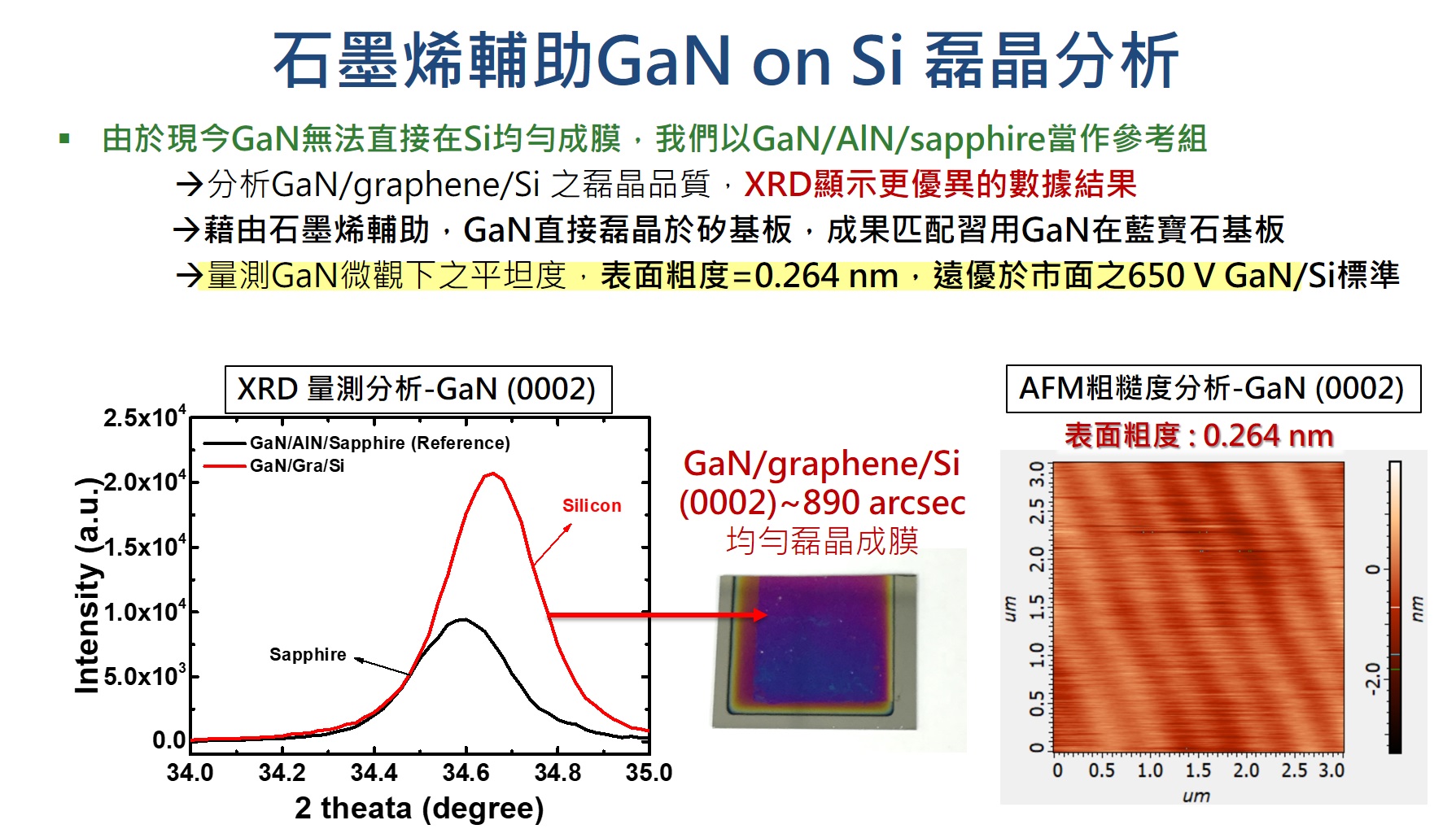
In this technique, it can synthesize high-quality and large area graphene. We develop batch to batch chemical vapor deposition (B2B-CVD) to reduce the cost to facilitate the industrialized production. At the same time, the development of high-quality six-inch graphene silicon wafers was made with our unique transferring process. The wafer can be used as epitaxial substrates, which can solve the bottleneck of poor heat dissipation of sapphire substrates, lattice mismatch of Si substrates, and expensive SiC and GaN substrates.
1. Use economical equipment integrated our patented high-density rolling method to achieve scale up synthesis of high quality and large-area graphene for industrialized production. When the reaction chamber diameter reaches 8 inches, the productivity can be increased to 6.7 m2/h, which can reduce the cost. 2. Ultra-high clean transfer printing process, so that the surface cleanliness meets the specifications for making electronic components. 3. The GaN epitaxy process is performed on graphene as the buffer layer on the Si substrate to obtain high-quality crystalline state.
The lattice structure of graphene has a good match with that of GaN, and it can be applied to epitaxial fabrication process. If high-quality graphene is transferred onto a silicon wafer for epitaxy, which can replace the conventional sapphire substrate for epitaxy. That can solve the bottlenecks of poor heat dissipation, lattice mismatch, and expensive SiC and GaN substrates encountered by conventional sapphire substrates. It can produce high-efficiency and cost-economic niche components, such as high-power/high-frequency electronic components, microwave components, short-wavelength LED/Laser.
線上展網址:
https://tievirtual.twtm.com.tw/iframe/a50c4e70-20fd-4534-8cc0-adaf4b795d25?group=23bfb1fa-dd5b-4836-81a1-4a1809b1bae5&lang=en
National Central University is a public research university with long-standing traditions of the Republic of China based in Taiwan. It was founded in 1902 and renamed in 1915. The school was initially located in Miaoli when it first moved to Taiwan, but relocated to Zhongli in 1962 and developed into a comprehensive university. It's the first university in Taiwan to research industrial economics,[3] and economic development (Taiwan's Consumer Confidence Index is released monthly by NCU).[4] NCU is a member of AACSB.[5] NCU is one of the six national universities in research selected by the Ministry of Education.
The innovative technology that turns waste into treasure – Silicon Dioxide regenerated from semiconductor waste that contains Silicon
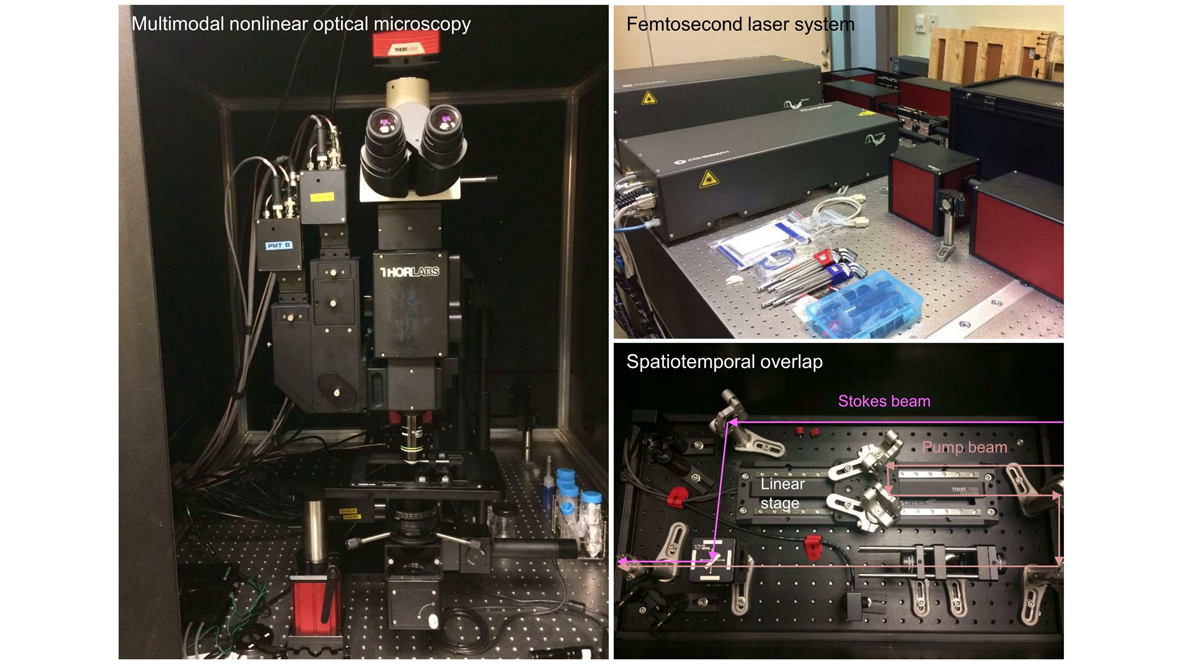
Multimodal nonlinear optical microscopy platform for the identification of artificial bone materials
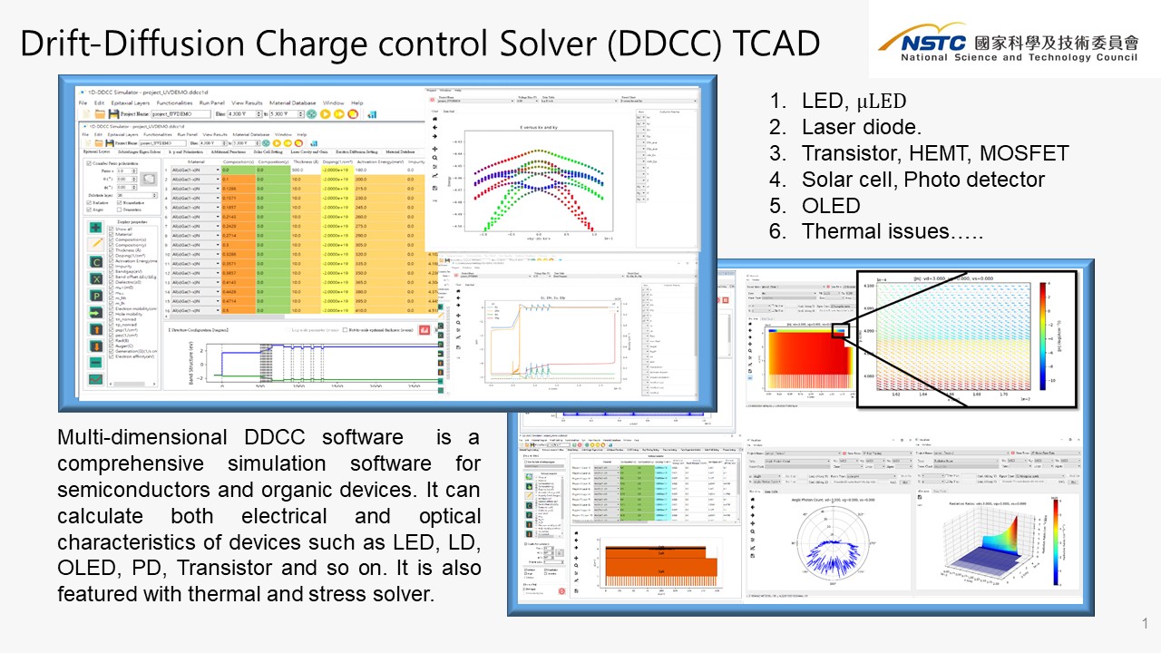
A Multi-Physics Coupled Simulation Platform for Next-Generation Wide-Bandgap Semiconductors (DDCC-TCAD)
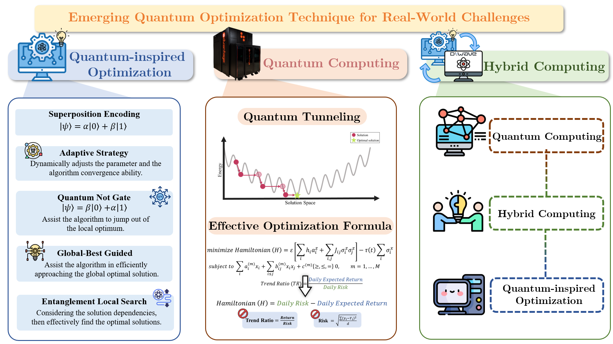
Innovative Hybrid Framework of Quantum-inspired Algorithms and Quantum Computing for Applications in Finance and Optimization Problems
Technology maturity:Experiment stage
Exhibiting purpose:Product promotion、Display of scientific results
Trading preferences:Technical license/cooperation、Negotiate by self
*Organization
*Name
*Phone
*Main Purpose
*Discuss Further
*Job Category
*Overall Rating
*Favorite Area
*Key Tech Focus
*Willing to Receive Updates?
Other Suggestions
Coming soon!