High gate reliability performance of normally-off p-GaN HEMT with AlGaN cap layer grown on a low-resistance SiC substrate.
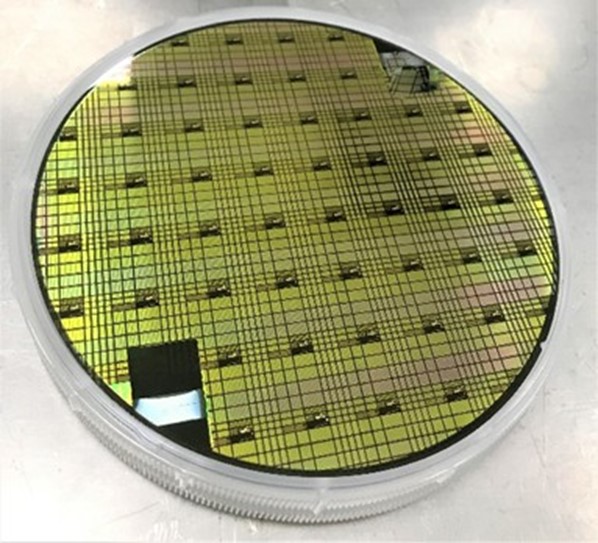

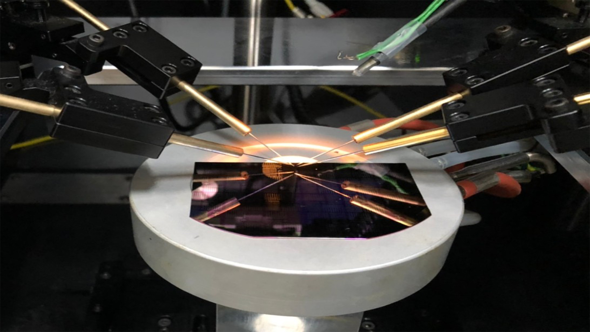
We grew p-GaN HEMT on a low-resistance SiC substrate and added a AlGaN cap layer above the p-GaN layer. We use the wide band gap material AlGaN as the cap layer, which can effectively suppress the holes injection and achieve the purpose of improving the gate reliability. In addition, we chose a zero-degree angle and low-resistance SiC substrate, which not only greatly reduces the lattice dislocation defects caused by the heterogeneous junction, but also greatly reduces the overall cost.
In this research, AlGaN cap and zero-angle and low-resistance SiC substrates are the first to be applied to p-GaN HEMT, and our team combined the two to successfully develop a new high-voltage, high-stability p- GaN HEMT structure.
We grew AlGaN on the p-GaN layer to reduce the hole injection effect and make the gate operation bias>20V. It is hoped that the gate driver of traditional silicon devices can be shared, and the operating safety voltage of the gate will be increased at the same time. In addition, we also grew p-GaN HEMT on a low-resistance and zero-degree SiC substrate, so that the GaN on SiC element can have a lower lattice defect density at the buffer layer position, improve heat dissipation performance, and better the quality of crystals, and there are also lower prices.
線上展網址:
https://tievirtual.twtm.com.tw/iframe/ac361b7e-3df9-4506-b2be-7b705be7cbd6?group=23bfb1fa-dd5b-4836-81a1-4a1809b1bae5&lang=en
Centering on biotechnology research and medical studies, Chang Gung University set up research centers in medicine, engineering, management and other related fields. Furthermore, the university integrates research resources from an array of research teams to achieve the best results. In addition, we apply high technology to our two main research themes "cross-platform precision medical strategy" and "comprehensive smart health care". Our goal is to develop a comprehensive smart health care “iHealthCare” system, so as to continue promoting interdisciplinary, international cutting-edge advanced research and cultivating talents. To develop a number of interdisciplinary research centers is another focus of the university. We have been working towards the establishment of interdisciplinary research centers, as well as integrating and coordinating each college’s expertise in various fields, including precision medicine, healthy aging, disease infection, biomedical engineering, data science, artificial intelligence, management, decision-making optimization, and long-term health care, etc. It is worth noting that research objectives in various fields in conjunction with artificial intelligence technology serve to guide teachers to participate in relevant research and industry-academia cooperation. We expect that such an approach could improve interdisciplinary cooperation and add value to research and its application.
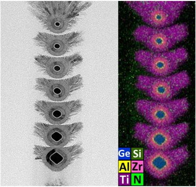
High mobility materials, process, stacked channels, and thermal circuit simulation; Ferroelectric X:HfO2 for Negative Capacitance and POC(Proof-of-Concept) Applications; Atomic layer technologies for
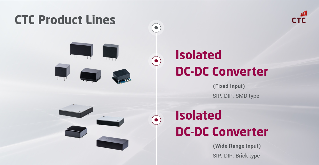
High-performance power conversion module with low no-load power consumption
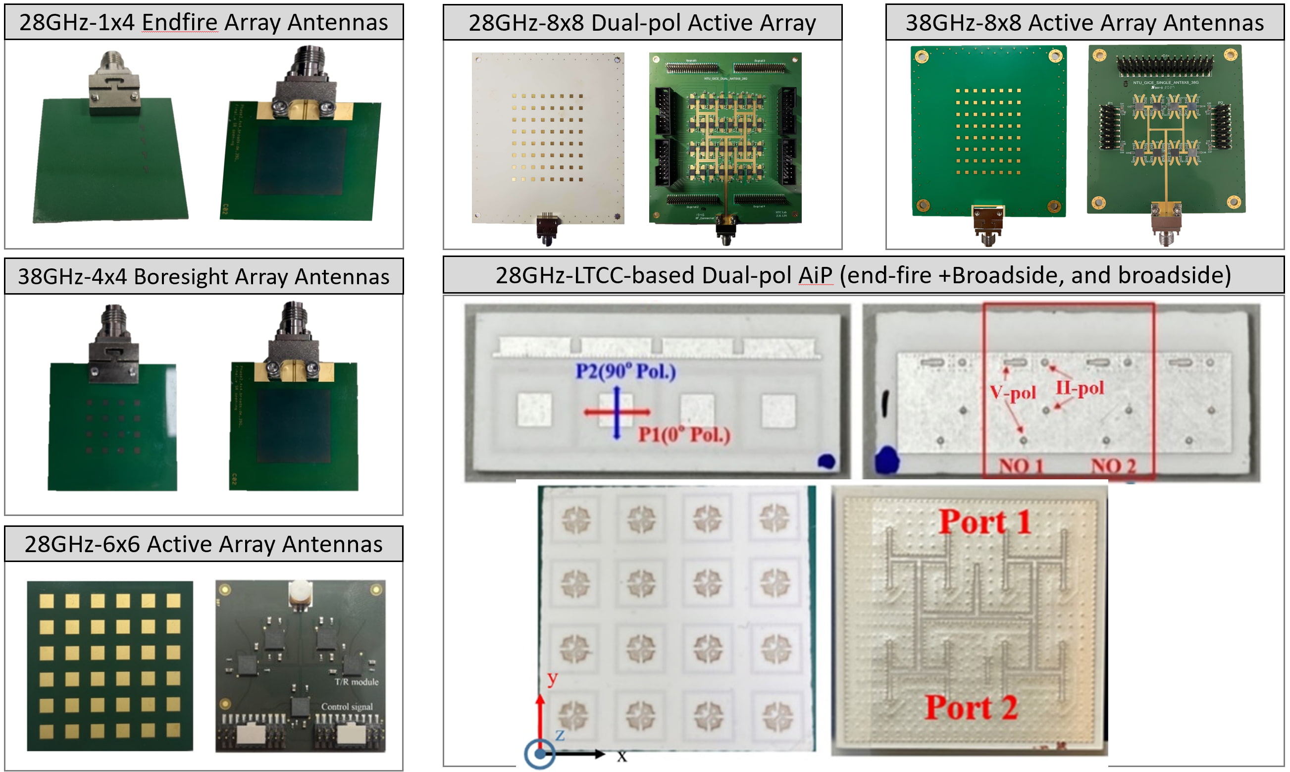
Antenna-in-package (AiP) Technology Suitable for Feeding to the Smart Impedance Material for High-Gain Radiations at Millimeter Wave Frequencies
Low Temperature Polycrystalline Silicon Oxide (LTPO) TFT Architecture with Memory-embedded in Pixel for High-resolution and Power-saving Near-eye VR/AR Displays Applications
Technology maturity:Experiment stage
Exhibiting purpose:Product promotion、Display of scientific results
Trading preferences:Technical license/cooperation、Negotiate by self
*Organization
*Name
*Phone
*Main Purpose
*Discuss Further
*Job Category
*Overall Rating
*Favorite Area
*Key Tech Focus
*Willing to Receive Updates?
Other Suggestions
Coming soon!