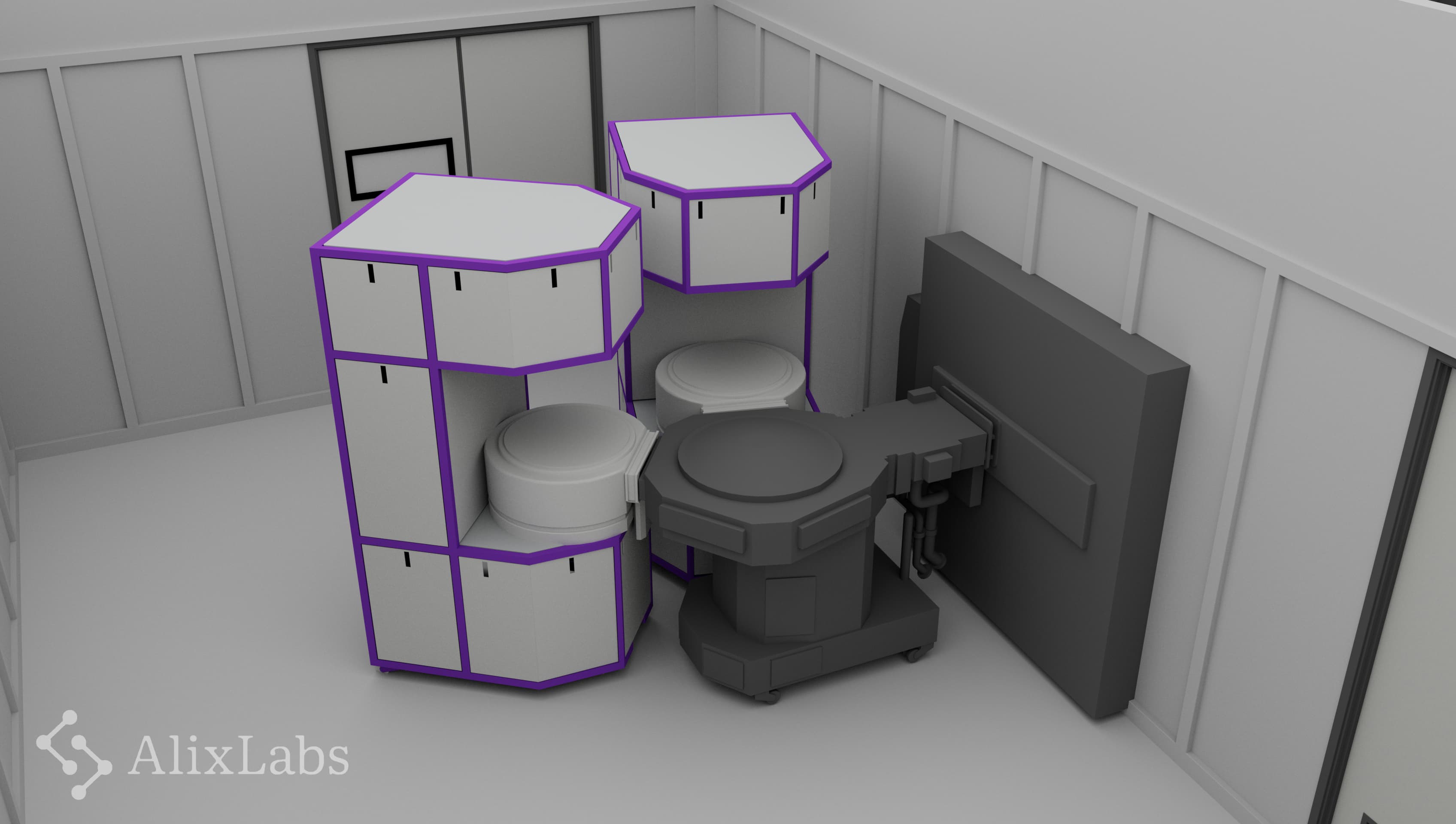
Atomic Layer Pitch Splitting: a breakthrough equipment solution for advanced semiconductor manufacturing.
Technology Introduction:
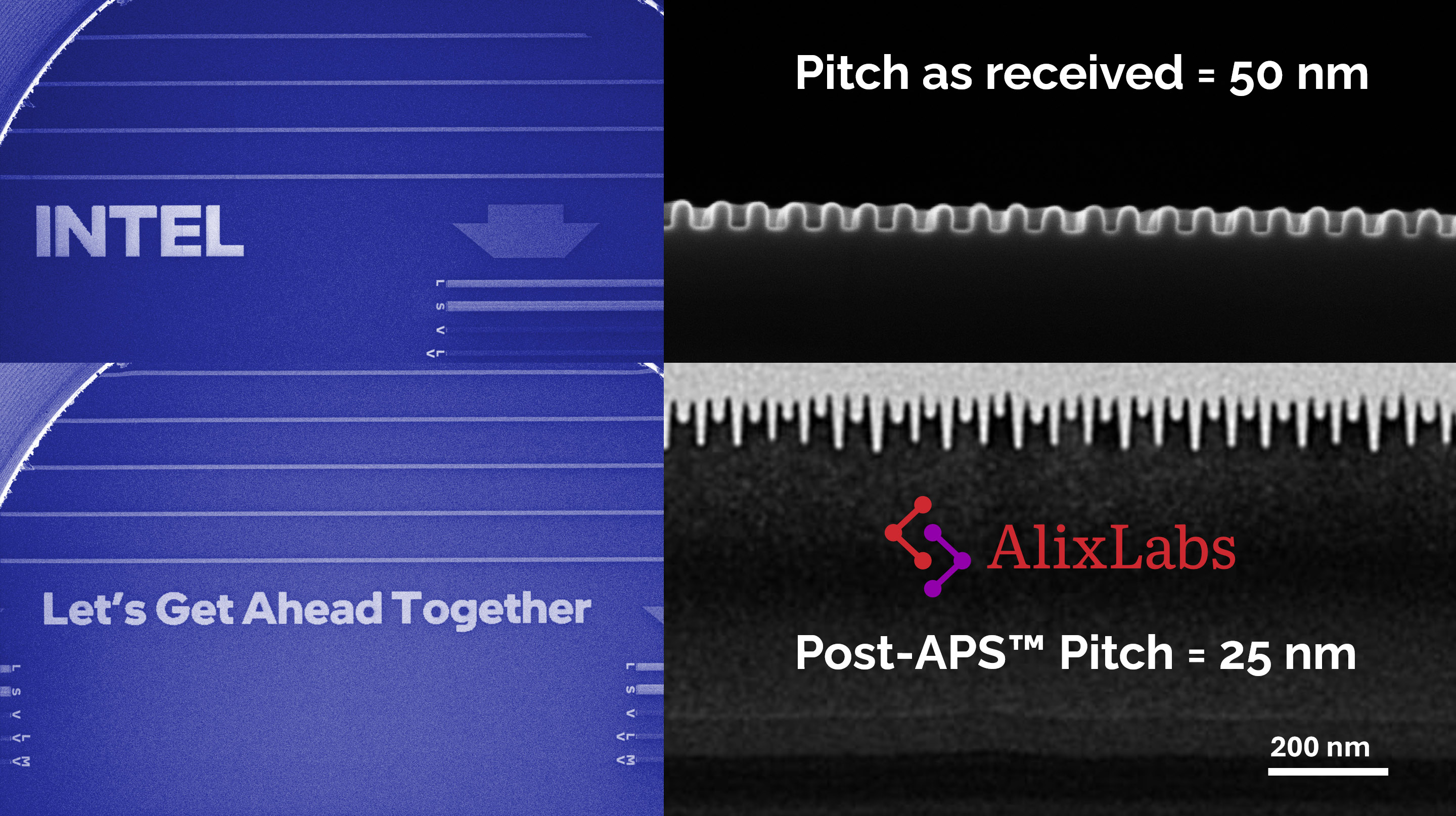
AlixLabs' unique and patented Atomic Layer Pitch Splitting (APS) is a novel plasma-based etching method that selectively targets surface topology. This breakthrough technology eliminates several complex steps in chip manufacturing, enabling more efficient, cost-effective, and sustainable semiconductor production.
Industry Applicability:
APS enables cost-efficient scaling of semiconductor devices by doubling pattern density. It reduces manufacturing costs, lowers energy use, and supports sustainable, high-volume production. Applicable in logic, memory, and power devices, APS accelerates industrial adoption with scalable chip manufacturing.
"AlixLabs is a Swedish semiconductor industry supplier with equipment and processes capable of manufacturing nanostructures with characteristic sizes smaller than 20 nanometers. We enable energy efficient fabrication of structures beyond the resolution limits of optical and electron beam lithography – through APS™."
16084992
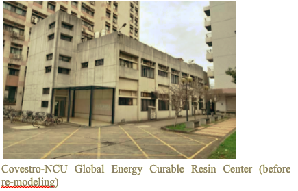
NCU-Covestro Research Center: Research and Development of Green Advanced Functional Materials and Manufacturing Processes
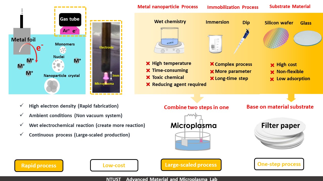
Three dimension nanoporous nanomaterial Microplasma-Enginnered assemblies on paper substrate for hydrogen gas production , surface-enhanced Raman scattering and catalytic reduction
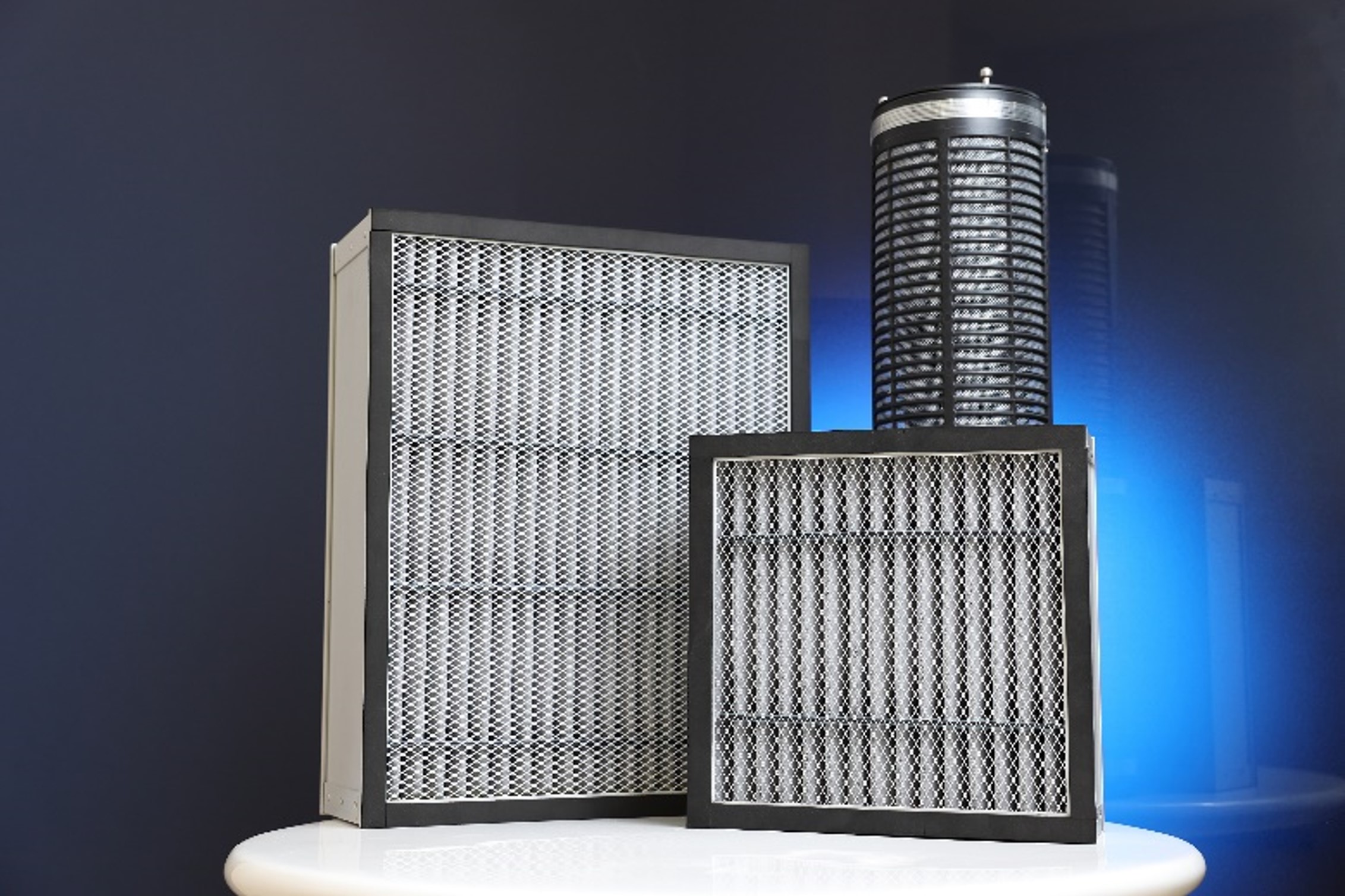
The world's first carbon-neutral regenerative filter: A Sustainable New Solution for Semiconductor Clean Air
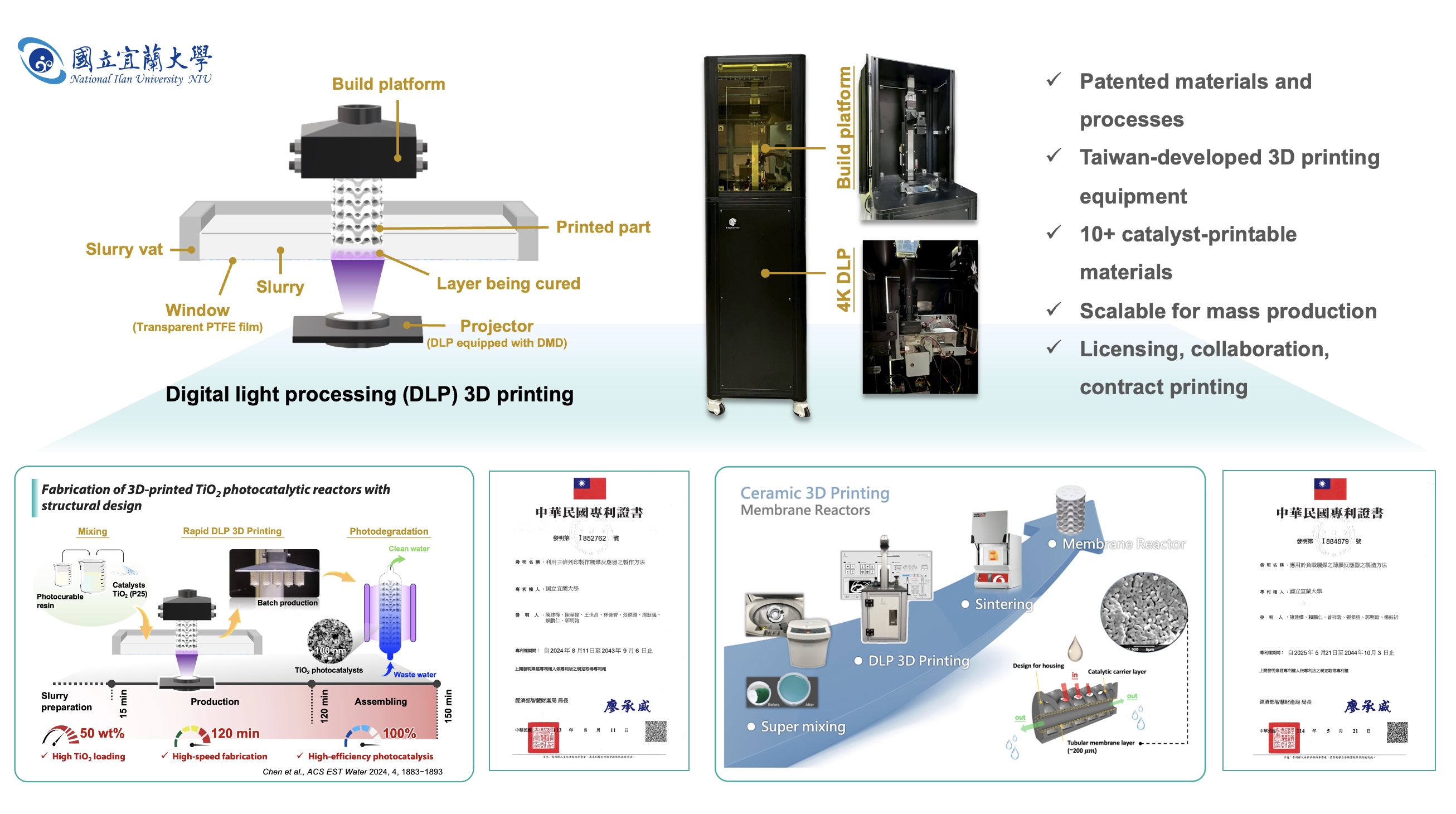
Scalable Catalytic 3D Printing Process Development: Enabling Smart Transformation in Chemical Reactor Bed Design and Manufacturing
Technology maturity:Prototype
Exhibiting purpose:Product promotion
Trading preferences:New products development
*Organization
*Name
*Phone
*Main Purpose
*Discuss Further
*Job Category
*Overall Rating
*Favorite Area
*Key Tech Focus
*Willing to Receive Updates?
Other Suggestions
Coming soon!