Scalable Catalytic 3D Printing Process Development: Enabling Smart Transformation in Chemical Reactor Bed Design and Manufacturing

Technology Introduction:
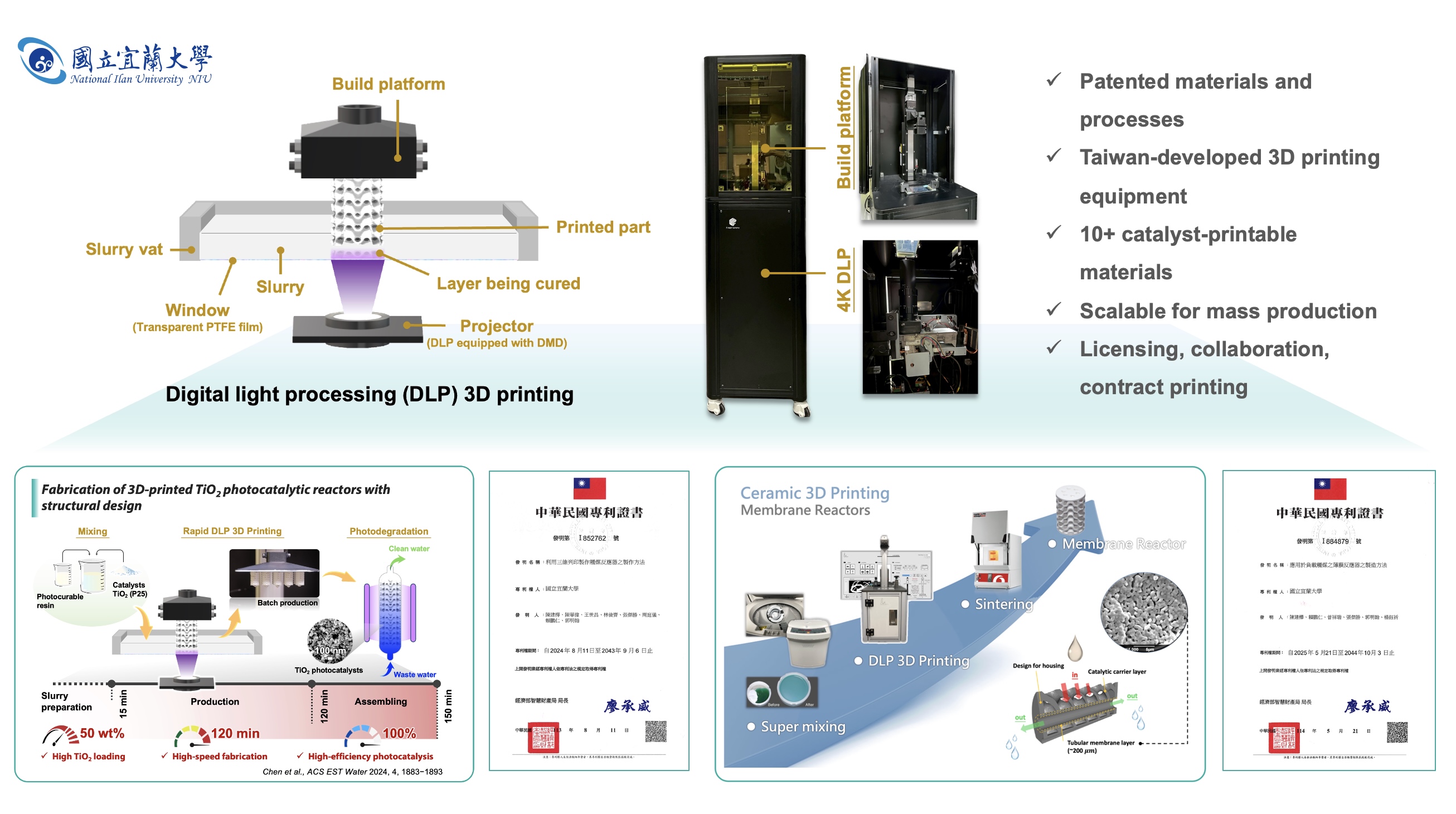
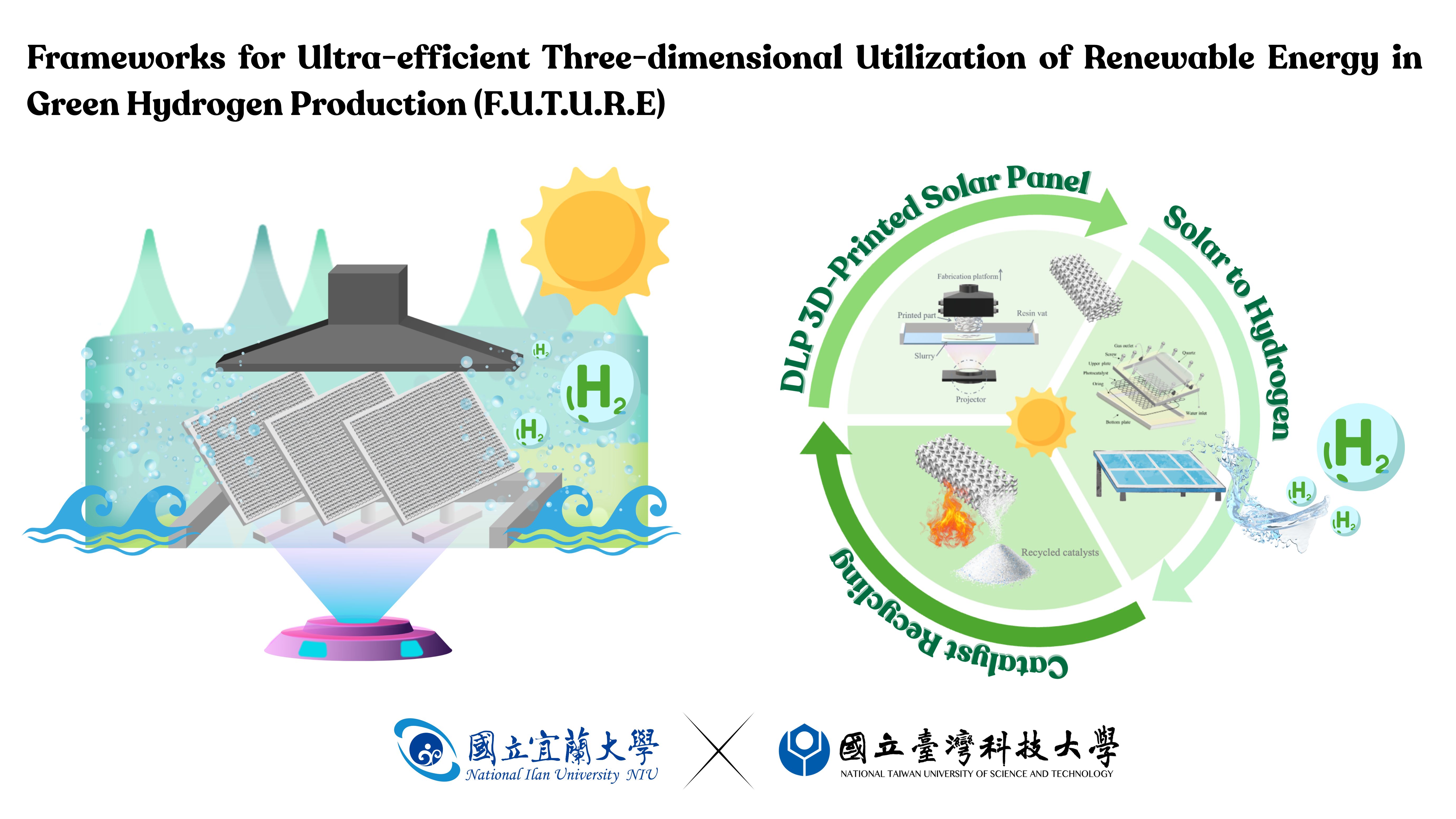
This technology enables a scalable 3D printing process for catalytic systems, featuring high solid-loading resins, topological structures, DLP printing, and post-processing to produce efficient reactor beds. Validated with TiO₂, zeolites, MOFs, metals, and ceramics, it supports hydrogen production, pollutant removal, and VOC control for net-zero applications. Integrated with AI and digital manufacturing, the process holds two invention patents and supports smart catalytic reactor deployment.
Industry Applicability:
This technology offers a scalable catalytic 3D printing platform with high solid-loading resins and integrated printing and post-processing. It supports TiO₂, zeolites, MOFs, metals, and ceramics. Standard and custom materials, modules, and contract manufacturing are available for research, chemical, and equipment sectors. With flexibility, scalability, and patents, it is applied in net-zero, hydrogen energy, and carbon capture, showing strong commercialization and global potential.
National Ilan University was one of the first institutions of higher education in Taiwan. It was founded as the Taiwan Provincial Ilan School of Agriculture and Forestry on 12 May 1926. Since then, the name and focus of the institution have undergone a number of changes, from having been a five-year junior college (National Ilan Junior College of Agriculture and Technology), and a polytechnic college (National Ilan Institute of Technology). In 2003, the school was further reformed into its current status as a comprehensive university, offering BA, BS, MA and MS degrees in four colleges.
I852762
NCU-Covestro Research Center: Research and Development of Green Advanced Functional Materials and Manufacturing Processes
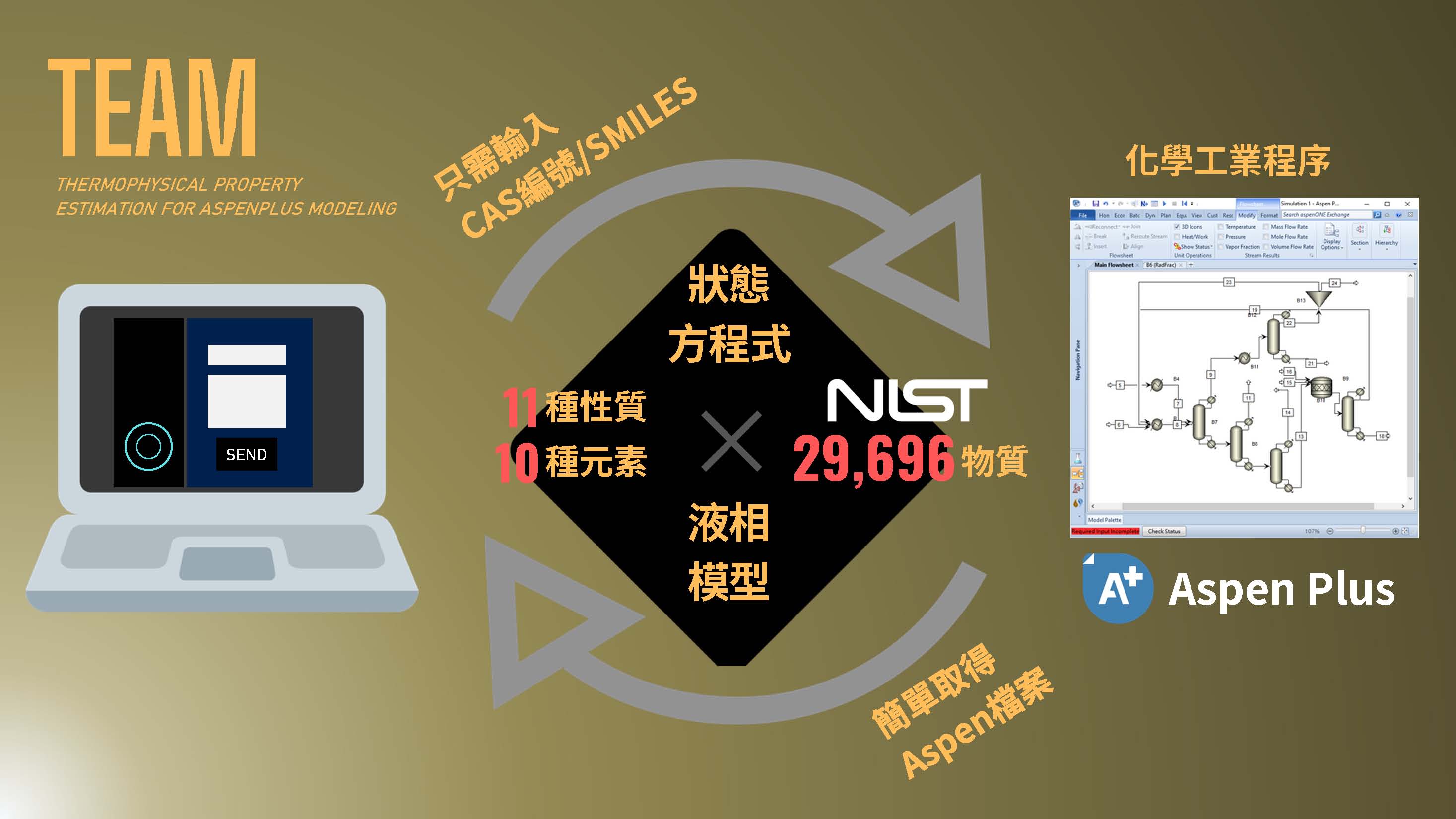
The Engine for Novel Chemical Engineering Process Development: a Fully Automated Platform for Comprehensive Physical Property Prediction
Development and system integration of compound semiconductors and advanced packaging technologies
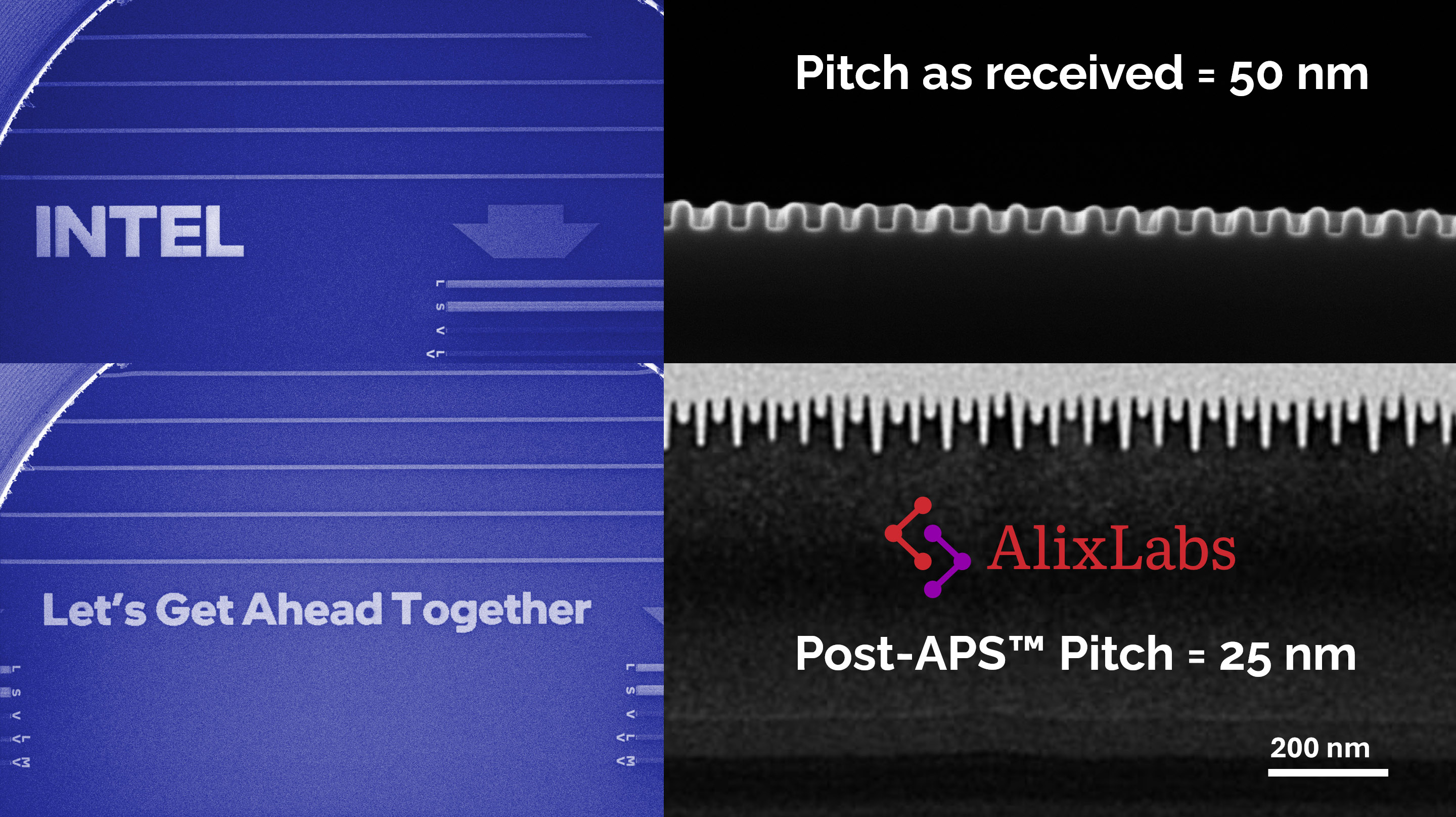
Atomic Layer Pitch Splitting: a breakthrough equipment solution for advanced semiconductor manufacturing.
Technology maturity:Others
Exhibiting purpose:Display of scientific results
Trading preferences:Negotiate by self
*Organization
*Name
*Phone
*Main Purpose
*Discuss Further
*Job Category
*Overall Rating
*Favorite Area
*Key Tech Focus
*Willing to Receive Updates?
Other Suggestions
Coming soon!