Development and system integration of compound semiconductors and advanced packaging technologies

To enhance the competitiveness of wide bandgap semiconductors (GaN and SiC) in Taiwan’s and Japan’s 5G/6G communications, automotive, and renewable energy sectors, the Academy of Innovative Semiconductor and Sustainable Manufacturing, in collaboration with Institute of Science Tokyo, is leading an integrated development plan. This initiative unites academia, industry, and research institutions from both Taiwan and Japan to strengthen their global semiconductor positions and develop future talent. By closely collaborating, the teams from Taiwan and Japan will optimize device performance and packaging solutions, aiming to position both countries as leaders in these critical technologies.
The college offers specialized degree programs including Chip Design, Semiconductor Process, Semiconductor Packaging and Testing, Critical Materials, and Intelligent and Sustainable Manufacturing. Each program has its own core and elective courses as well as distinct academic culture, yet they are closely interconnected, encouraging students to take courses across programs to cultivate both specialized semiconductor expertise and broad technological leadership skills. These programs cover the upstream, midstream, and downstream sectors of the semiconductor industry. Courses are designed to integrate into modular teaching units, and faculty expertise can be combined to develop forward-looking research topics. The curriculum incorporates Artificial Intelligence (AI), Big Data Analytics, Internet of Things (IoT), Smart Manufacturing, Sustainable and Circular Practices, Green Technology, and Carbon Neutrality, providing students with comprehensive training beyond semiconductor specialization to meet the needs of future technologies.

High temperature and corrosion resistant SiC susceptor for compound semiconductor process
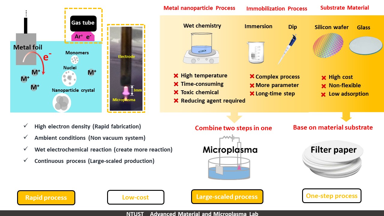
Three dimension nanoporous nanomaterial Microplasma-Enginnered assemblies on paper substrate for hydrogen gas production , surface-enhanced Raman scattering and catalytic reduction
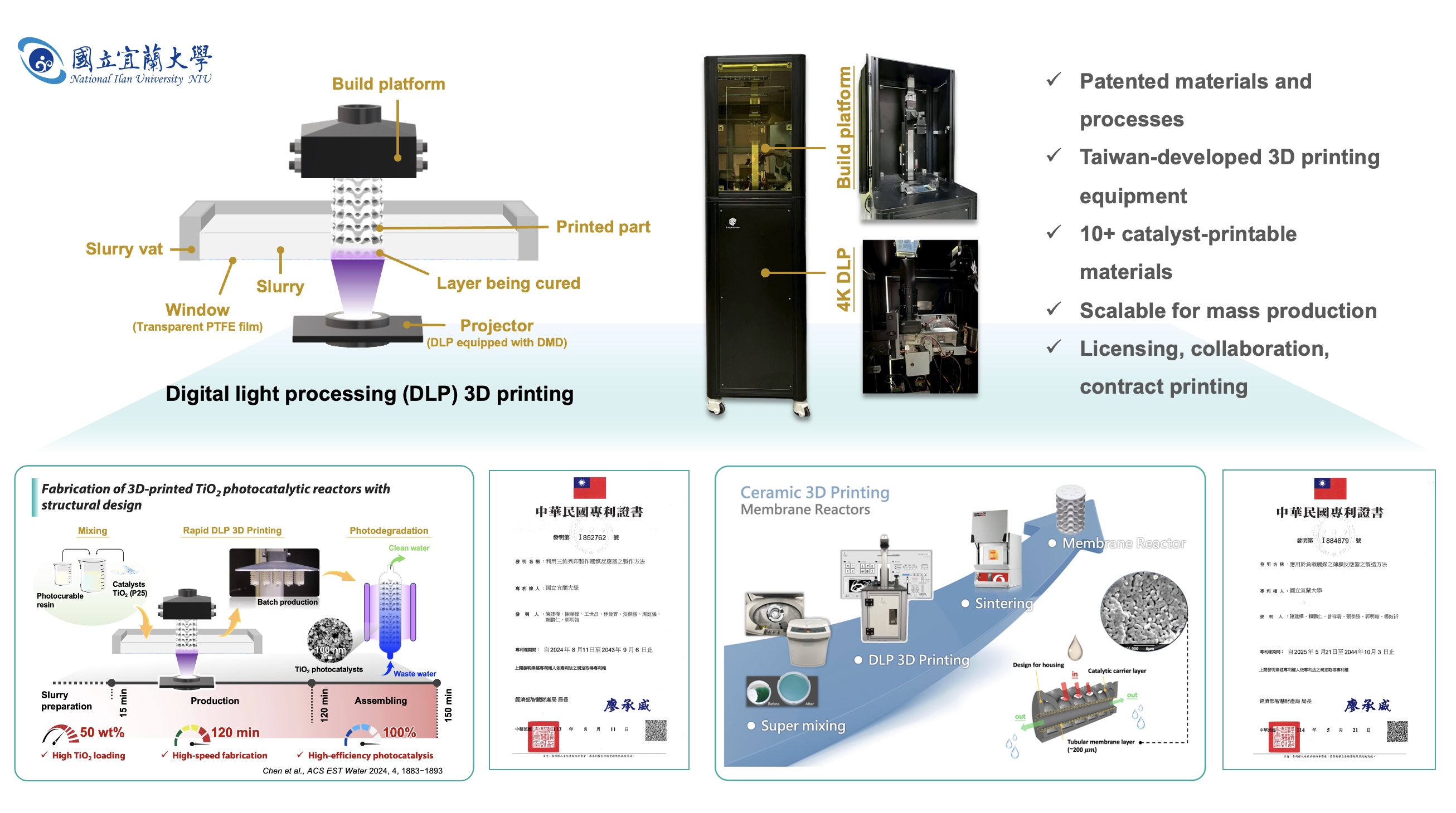
Scalable Catalytic 3D Printing Process Development: Enabling Smart Transformation in Chemical Reactor Bed Design and Manufacturing

Atomic Layer Pitch Splitting: a breakthrough equipment solution for advanced semiconductor manufacturing.
Technology maturity:Experiment stage
Exhibiting purpose:Display of scientific results
Trading preferences:Negotiate by self
*Organization
*Name
*Phone
*Main Purpose
*Discuss Further
*Job Category
*Overall Rating
*Favorite Area
*Key Tech Focus
*Willing to Receive Updates?
Other Suggestions
Coming soon!