Select Field
Select Ministry
13 results
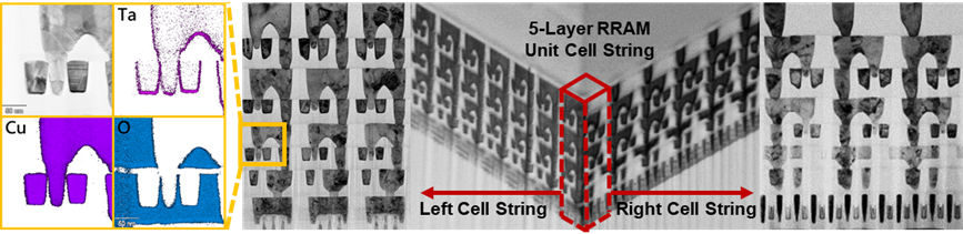
Technology Introduction: With the progress of AI and IoT, the demand for NVM in edge computing has increased. This project proposes a 3D high-density Via RRAM architecture compatible with advanced FinFET logic process. Featuring full integration to CMOS process, 3D stackability, and high density, the design demonstrates excellent stability, low power consumption, and fast operation through comprehensive device design and electrical validation, making it a promising solution for future embedded memory applications. Industry Applicability: The 3D Via RRAM is fully compatible to TSMC standard logic process. It has been demonstrated on the 16nm FinFET platform, achieving a density of 0.4 Gb/mm², exceeding international benchmarks with scalability toward 1 Gb/mm² at 7nm node. Featuring high reliability, fast operation, and stable retention, this logic NVM IP is suitable for AI, IoT, and embedded system application. It shows strong potential for technology transfer, offering contribution to next-generation semiconductor technologies.
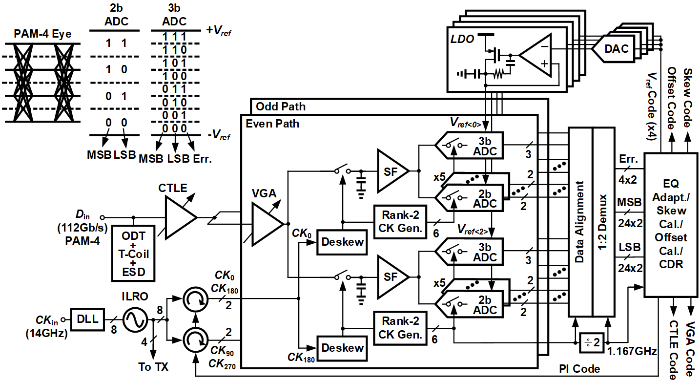
Future Tech | Electronics & OptoelectronicsTechnology Introduction: CPOs integrate the switch chip and modules on the same board, reducing size and distance. This achieves a Nyquist loss of <10dB at 28GHz for 112Gb/s PAM-4 signals. The focus is on a low-power 112Gb/s PAM-4 XSR RX using a 2b/3b TI-ADC. Time-interleaving removes high-speed comparators, allowing a low-speed SAR ADC to be efficient. Replacing some 2-bit ADCs with 3-bit ADCs improves signal alignment. The TX features an unsegmented FFE driver, enhancing bandwidth and reducing power consumption. Industry Applicability: This technology has multiple patents in the U.S. and Taiwan, indicating strong industrial potential. The commercialized model licenses the TX and RX architecture to IC design houses, maximizing royalty revenue through non-exclusive agreements. Moreover, we can provide the design files and layout for the 112Gb/s PAM-4 TRX chip, validated at 28nm, as high-speed SerDes IP. Other related technologies, such as front-end circuit design, CDR and adaptive equalization algorithms, can also be licensed.
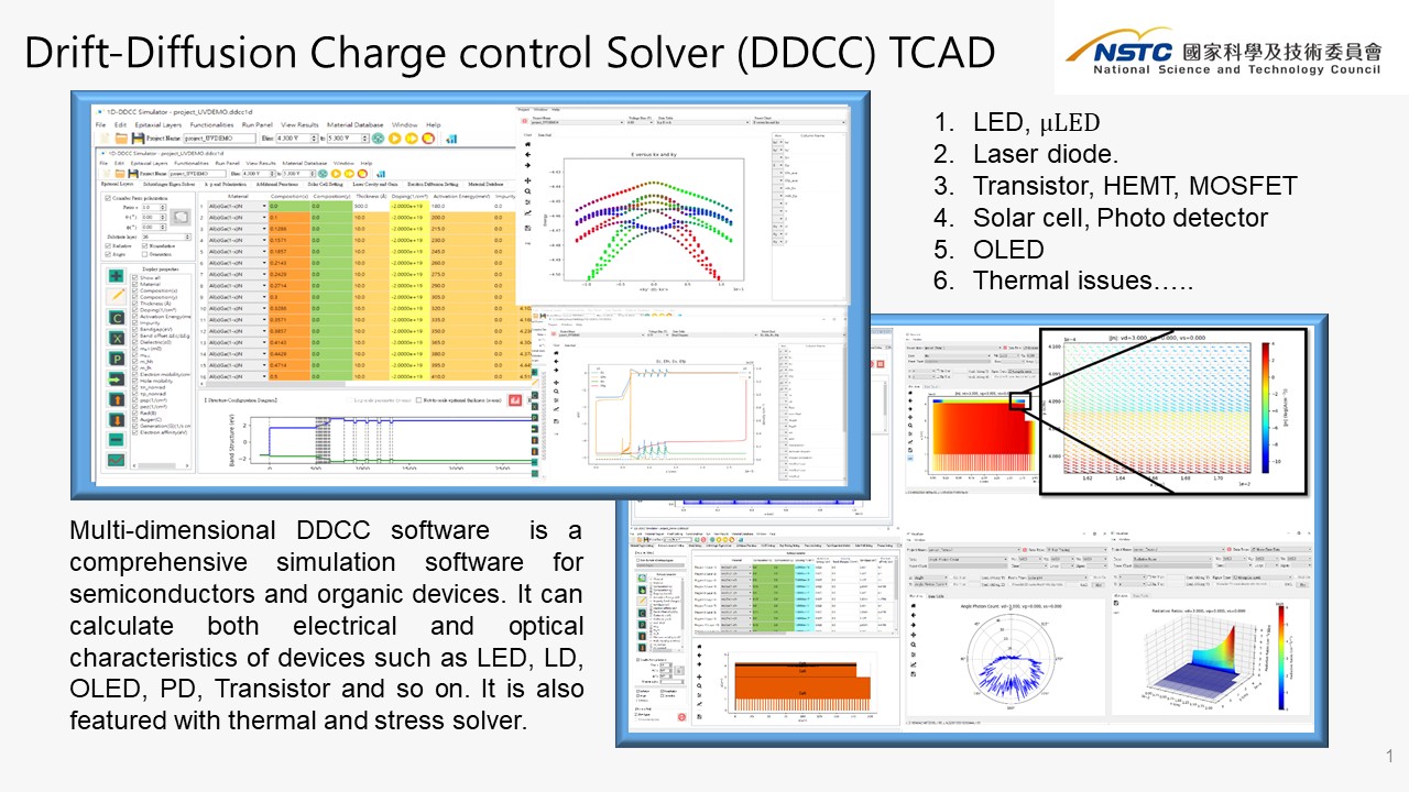
Future Tech | Electronics & OptoelectronicsTechnology Introduction: To accelerate next-gen semiconductor R&D, our team developed DDCC-TCAD, a fully autonomous multi-physics simulation platform. It pioneers the integration of the Localized Landscape (LL) theory, boosting computational efficiency by 1000x to accurately model quantum effects and solve key material disorder challenges. Commercially licensed by industry leaders like Apple and Meta device devepment department, and downloaded by over 1,000 academics worldwide, DDCC-TCAD has proven its high industrial and academic value. Industry Applicability: Our platform offers a versatile digital twin solution rivaling commercial software. Its unique Localized Landscape (LL) model provides superior physical insights. The technology's value is proven by commercial licensing to industry leaders like Apple and Meta, generating significant royalties. Critically, this autonomous platform breaks the foreign monopoly, ensuring Taiwan's strategic security and technological sovereignty in the semiconductor industry.
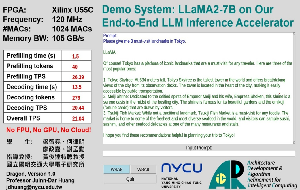
Future Tech | Electronics & OptoelectronicsTechnology Introduction: Our team developed MMA, a high-efficiency accelerator optimized for Transformer architecture and LLM inference. Featuring low power consumption and high performance, it is currently the only solution capable of fully running LLMs on edge devices. Compared to Georgia Tech’s MicroScopiQ, Seoul National University’s Tender, and Korea University’s OPAL, our design is the first to fully realize the vision of LLM on Edge, making secure and real-time AI possible. Industry Applicability: LLMs like ChatGPT are widely used in daily life. Our chip design enables real-time LLM inference without relying on the cloud or GPUs, reducing energy use and protecting data privacy. Imagine a future where anyone can run an LLM directly on their smartphone, or interact with a compact personal chatbot anytime, anywhere, completely offline and without worrying about data leaks. The solution not only enhances convenience but also resolves concerns around privacy, bringing AI into everyday life.
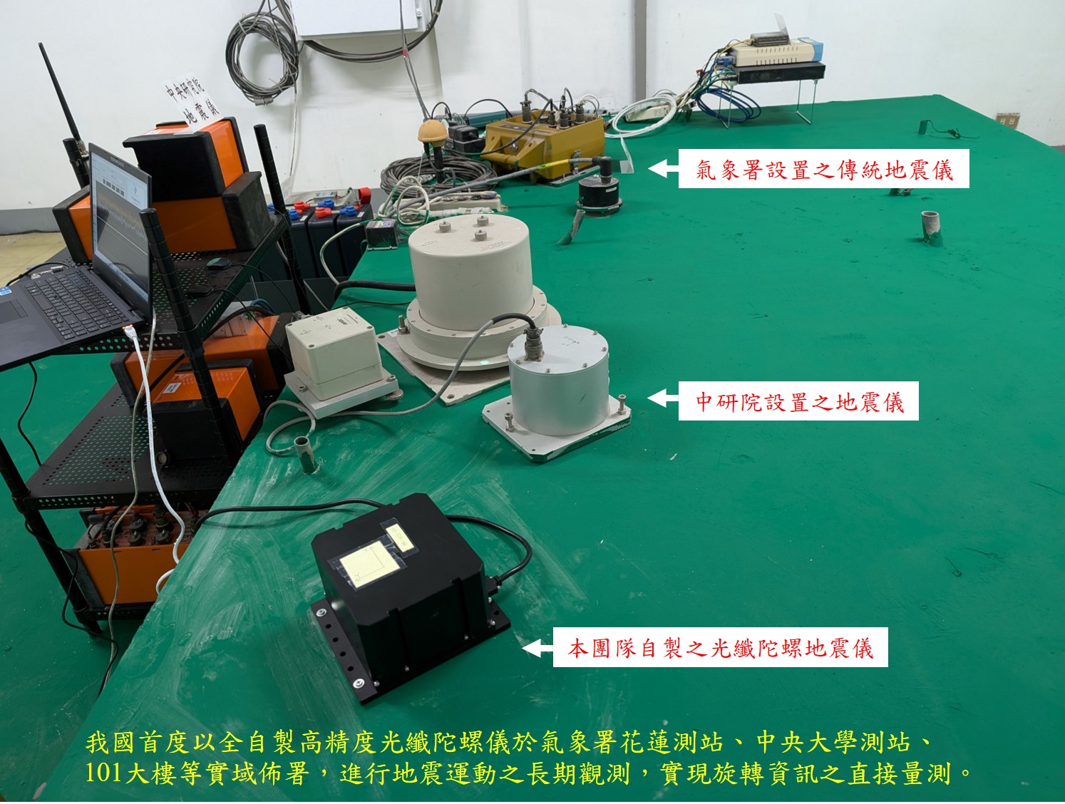
Future Tech | Electronics & OptoelectronicsTechnology Introduction: Rotational seismology is a key technology for advancing multidimensional and high-precision seismic sensing. This technology is focused on a self-developed FOG, establishing a sensing system for the rotational motions of seismic waves and enhancing both the dimensionality and accuracy of earthquake sensing. The FOG seismometer features high-precision rotational measurement, interference resistance, portability, and scalability, showing capabilities to build advanced seismic monitoring networks. Industry Applicability: The developed FOG seismometers not only advance research in seismology but also hold significant industrial values, including earthquake monitoring, civil engineering, automation, vibration protection for such as semiconductor fabs, energy, defense, aerospace, geological exploration, and smart disaster prevention. Our team aims to promote its application in smart sensing, unmanned vehicles, and low Earth orbit satellite industries through technology transfer and academia-industry collaboration.
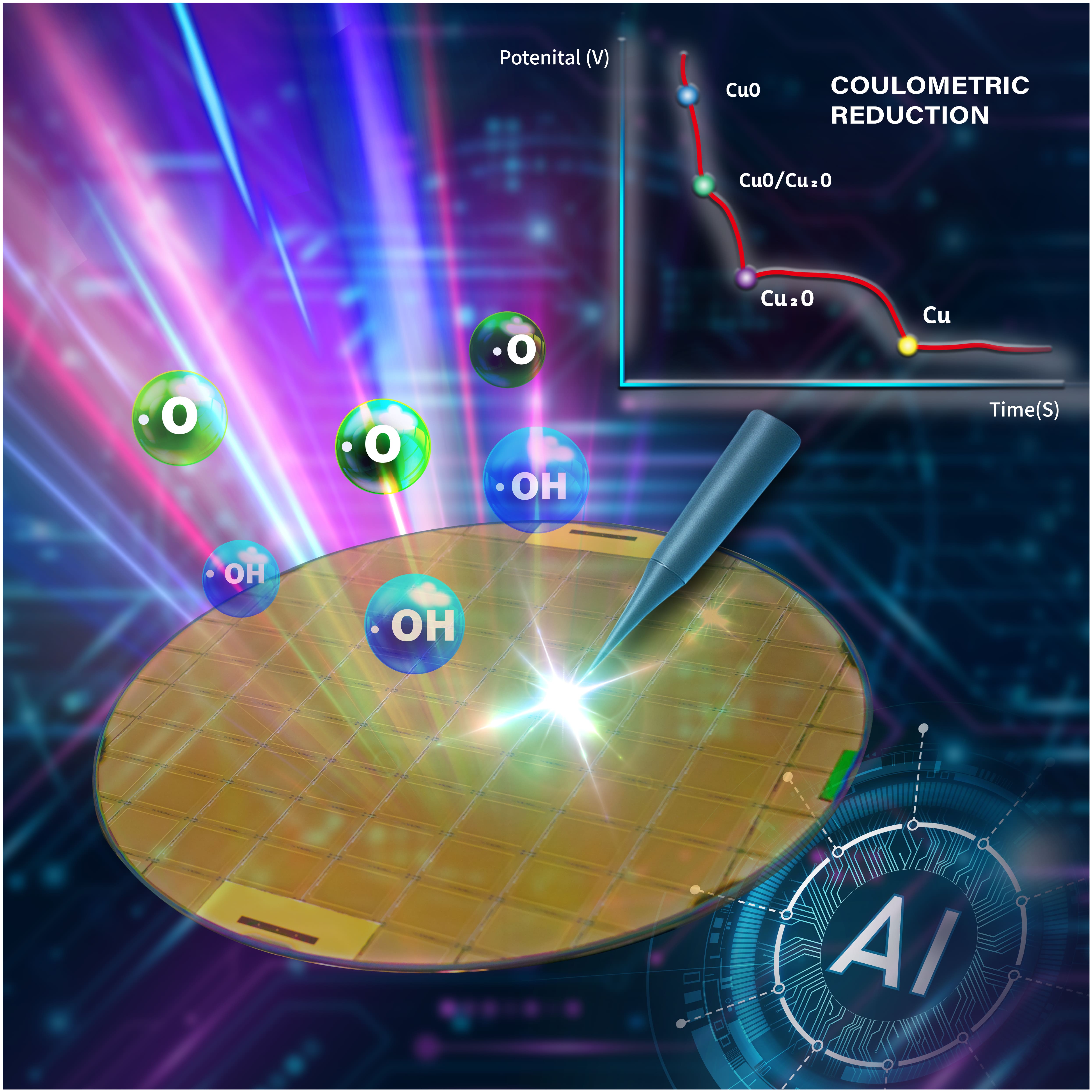
Future Tech | Electronics & OptoelectronicsTechnology Introduction: This project develops a 3D packaging bonding solution and smart platform integrating light-based surface treatment, mini electrochemical sensing, and AI prediction. It enables real-time analysis of copper oxidation and estimation of Cu–Cu bonding strength. Featuring portability, vacuum-free and non-destructive operation, and real-time feedback, it enhances yield, efficiency, and stability. The technology offers strong potential for next-generation semiconductor manufacturing. Industry Applicability: This technology targets key 3D packaging processes such as hybrid bonding in heterogeneous integration, replacing plasma treatments by enabling copper diffusion without vacuum. With integrated mini electrochemical sensing and AI prediction, it enables real-time oxide monitoring and automated control. The approach improves bonding strength and yield, offering high compatibility, scalability, and strong potential for commercialization and production deployment.
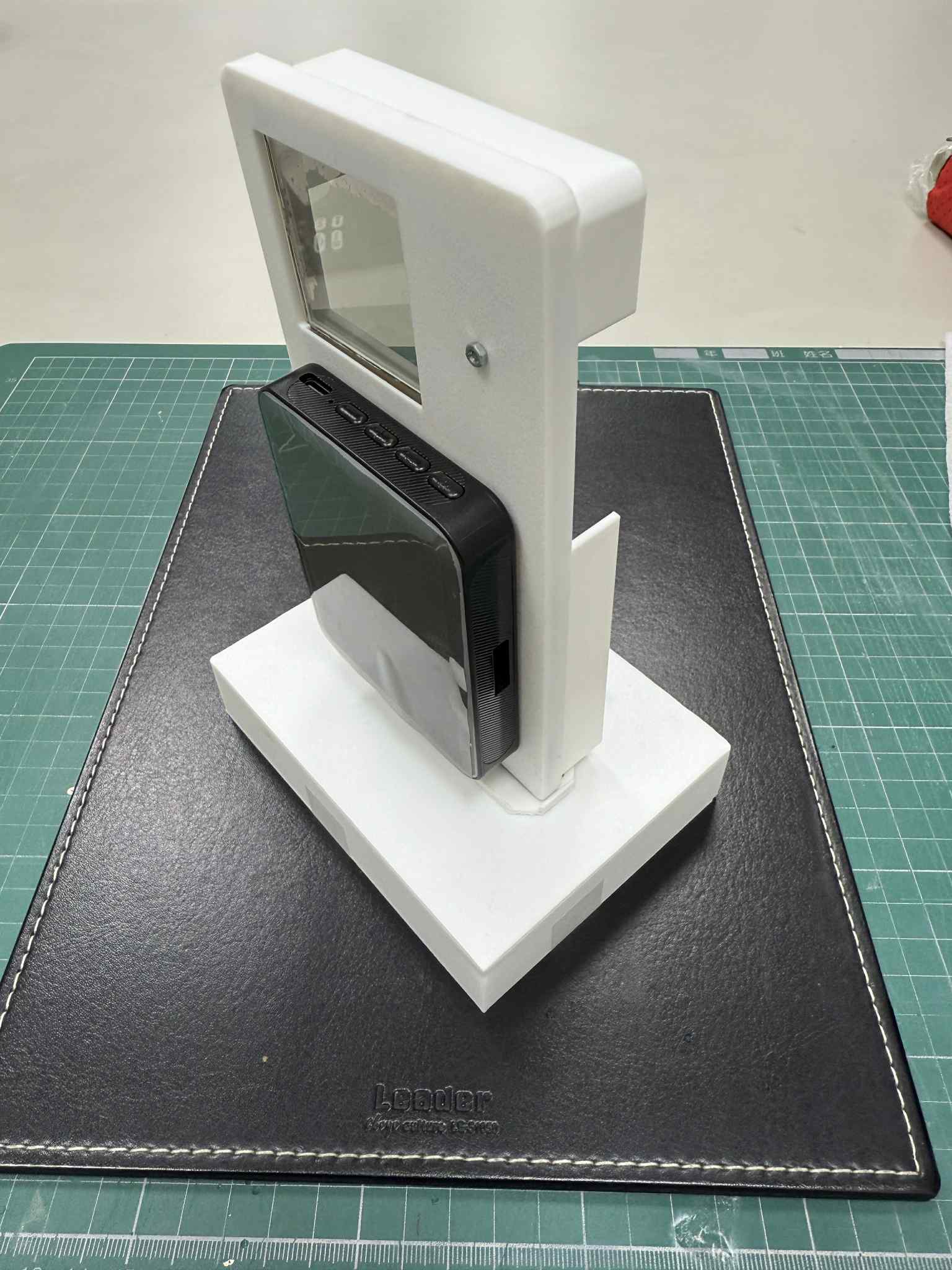
Future Tech | Electronics & OptoelectronicsTechnology Introduction: This system integrates skin analysis into a phone, using a liquid-crystal polarization modulator that switches polarization states in milliseconds to capture polarized images in 0.1 seconds. The app corrects any image misalignment, applies color-space conversion to enhance microvessels and pigment spots, and automatically marks acne, fine lines, and pores—calculating their counts and area. With just a smartphone and this clip-on case, users gain professional-grade, deep-layer skin insights. Industry Applicability: This system provides deep-layer detection technology to pure-software providers via API/SDK licensing, while enabling skincare brands and beauty studios to rapidly adopt through a hardware rental plus subscription model. The dual revenue approach blends licensing fees with recurring rental and subscription income, and leverages data monetization and aftermarket support to build a sustainable growth ecosystem.
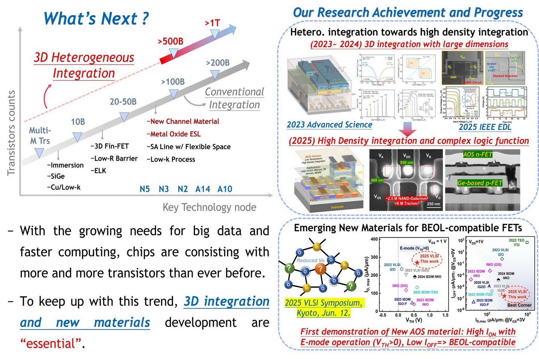
Future Tech | Electronics & OptoelectronicsTechnology Introduction: By leveraging a mature 100 nm process to replace sub-16 nm advanced nodes, this technology successfully integrates Ge-based p-FETs with In-based n-FETs featuring nanoscale channel thickness, achieving 2M NAND/mm² and moving toward the target of 20M NAND/mm² (80M Trs/mm²). In addition, this team pioneered a high-performance InWSnO transistor with an ultra-high on/off ratio and low subthreshold swing (SS), demonstrating strong potential for AI and HPC chip applications. Industry Applicability: This proposed 3D-IC achieves a world-leading transistor density and enabling logic circuits up to 8M Trs/mm² with a mature 100 nm-node process, instead of advanced several nm-node one. The core technology has been granted a Taiwan patent and a U.S. patent, demonstrating high commercialization potential. This work also pioneered the InWSnO TFT development, featuring excellent electrical performance, forming a key foundation for advancing next-generation 3D-IC technology.
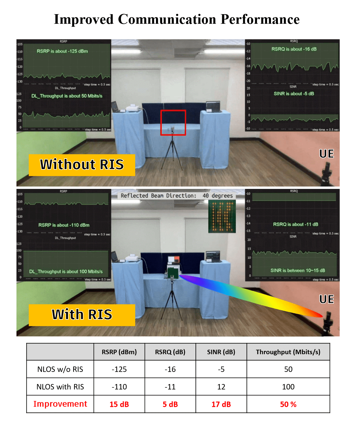
Future Tech | Electronics & OptoelectronicsTechnology Introduction: Our AI-native 6G RAN system with RIS and AI integration optimizes smart city wide-area connectivity. RIS enhances signal coverage and quality, while the 6G RAN RIC uses AI/ML for real-time network adaptation. The system improves coverage, communication quality, and energy efficiency, providing robust support for smart city development. Industry Applicability: RIS-assisted AI-native 6G RAN technology provides an innovative, low-cost, and eco-friendly solution for 6G mobile communications, addressing high construction and maintenance costs. It reduces power consumption (30%-90%) and carbon emissions while enhancing communication quality and system capacity. This technology promotes smart city development by offering efficient, reliable, and secure wide-area connectivity support for applications such as smart transportation, healthcare, and energy.
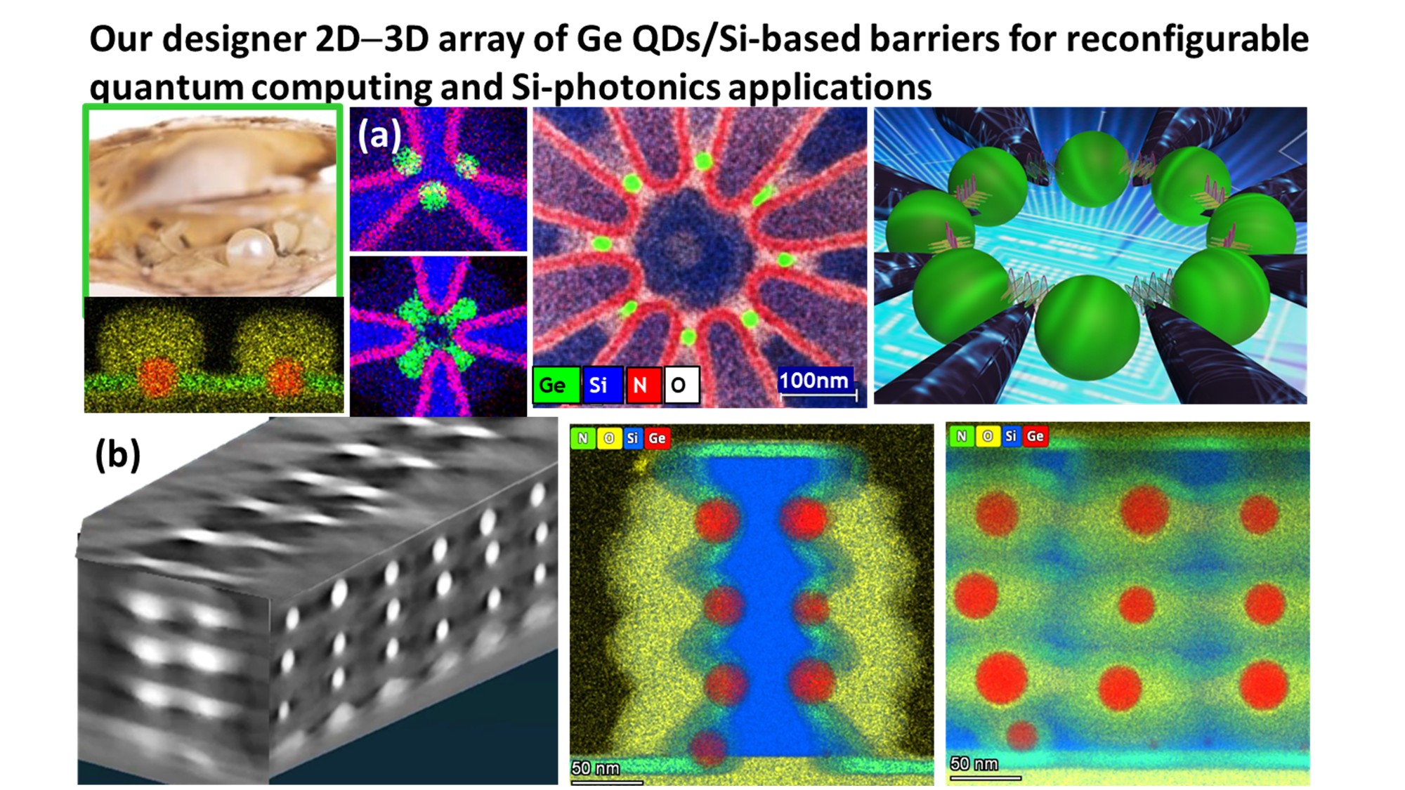
Future Tech | Electronics & OptoelectronicsTechnology Introduction: We report scalable architectures of Ge quantum-dots (QDs) using CMOS processes. Our QDs feature controllability, reproducibility, and scalability in size, morphology and position, creating a novel portfolio of quantum photonic and computing devices for manufacturing. We have demonstrated the first examples of Ge-QD SHTs operation at room temperature, double-QDs qubits operation at T > 10 K, and integration of SiN waveguided Ge photonics for on-chip optical interconnect and green computing. Industry Applicability: "From lab to fab is the driving force of our research team. Our CMOS integrable Ge qubits technology offers great promises for manufacturable semiconductor qubits operating at high temperatures and has gained tsmc and Metak interests. Our Ge QD technology is recognized for paving a promising and seminal route to achieve a key goal of Si photonic integrated circuits. Armed with our Ge quantum-dot technology, we hope to pave the way for a quantum leap for Taiwan's ICT industry."
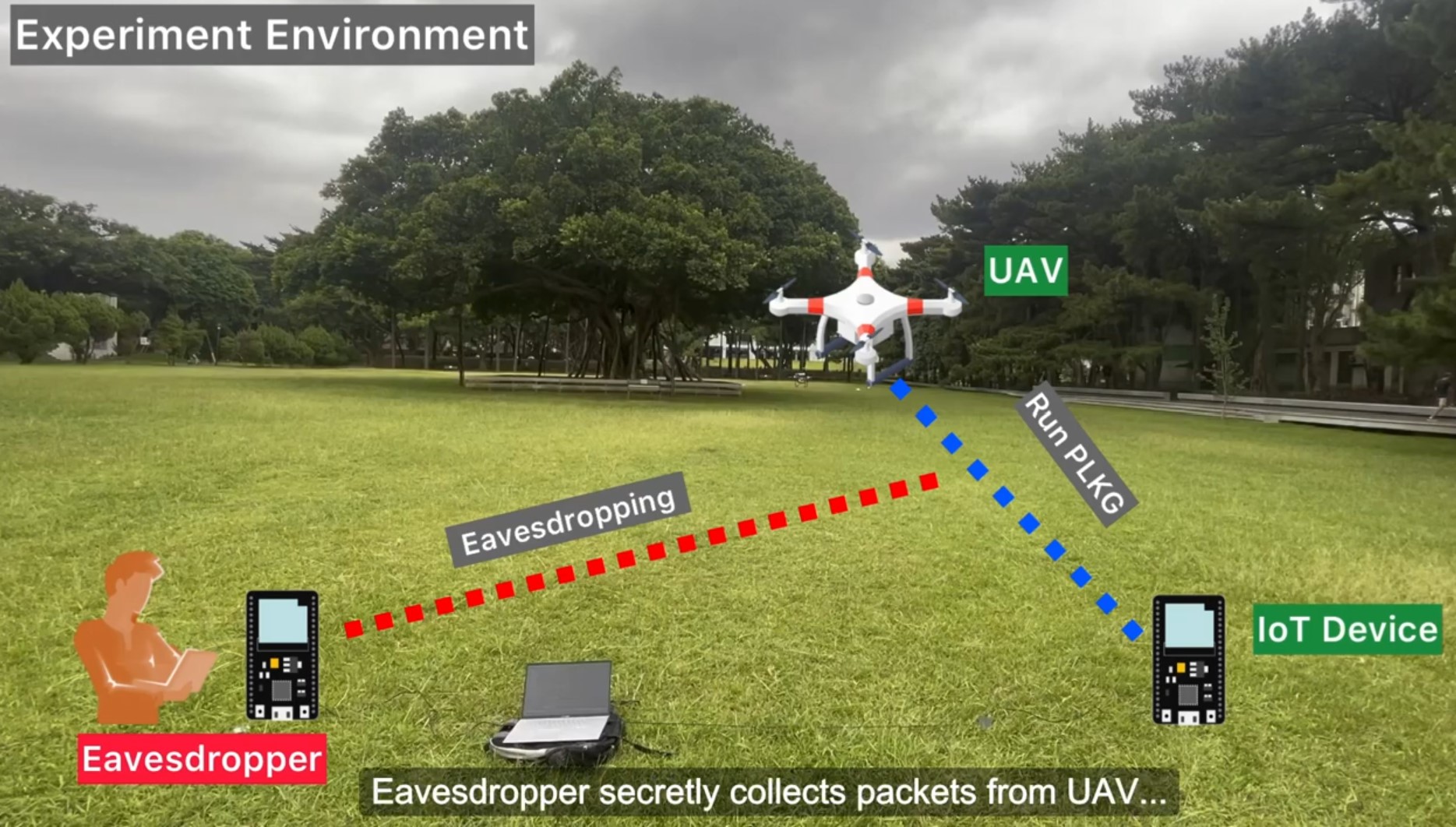
Future Tech | Electronics & OptoelectronicsTechnology Introduction: We propose a multimodal learning framework that integrates wireless channel state information with UAV flight trajectories to enhance the stability and security of physical layer key generation using deep learning models. The proposed technique effectively defends against future quantum decryption threats and is particularly suitable for environments with limited computational resources and the absence of trusted third-party authentication, thereby strengthening data protection in UAV networks. Industry Applicability:
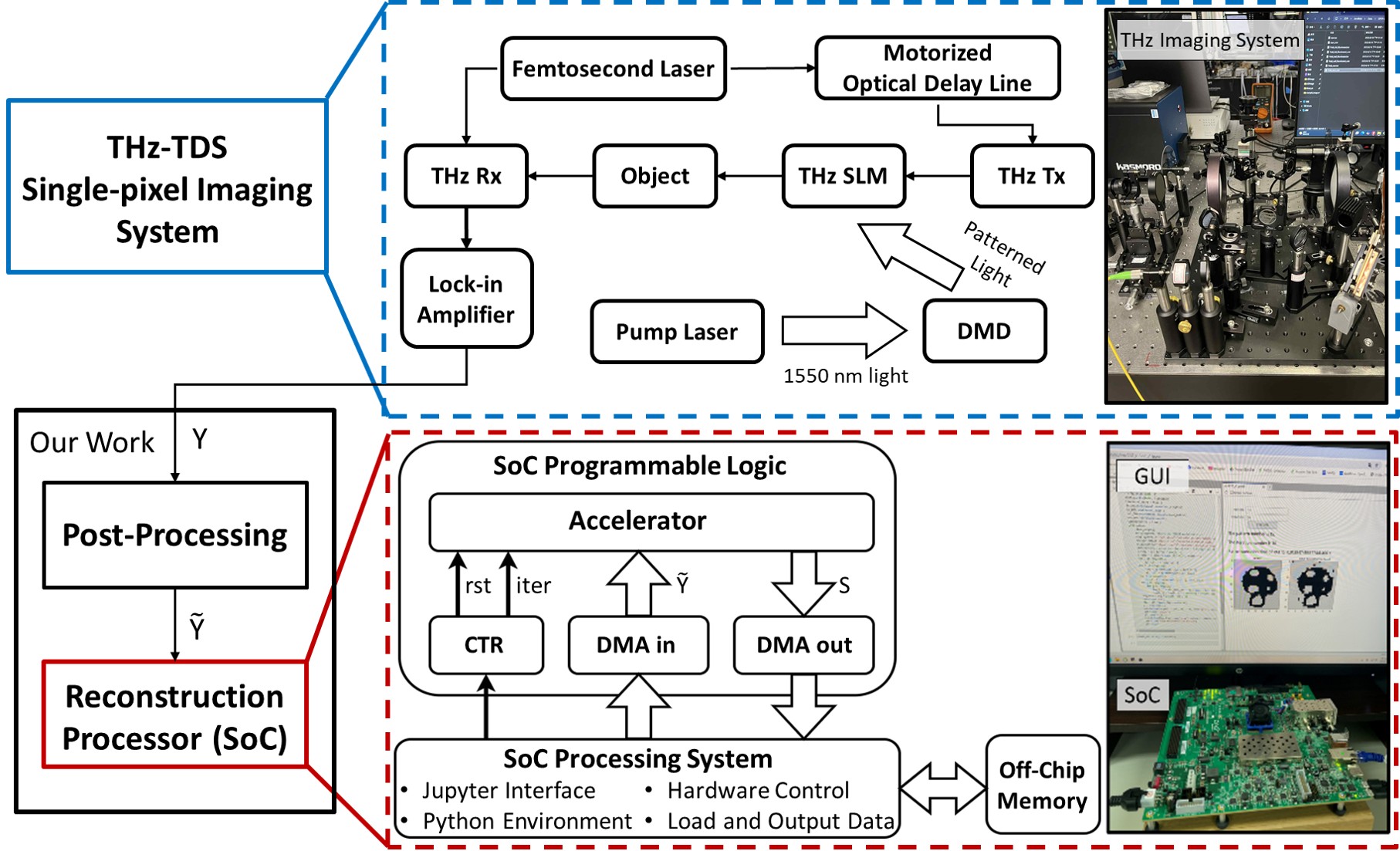
Future Tech | Electronics & OptoelectronicsTechnology Introduction: This project presents a terahertz single-pixel imaging system with high SNR and bandwidth based on a pulsed photoconductive antenna and a photoconductive spatial light modulator. A 3D tensor-based compressed sensing model compresses terahertz responses in spatial and temporal domains, preserving full waveform information for semiconductor material identification. The SOC system integrates an FPGA-based 3D imaging accelerator, enabling real-time refractive index imaging for material analysis. Industry Applicability: The FPGA/SoC-based THz single-pixel compressive sensing system delivers a breakthrough: high-speed, high-quality spectroscopic imaging. This unlocks crucial industrial applications: precise non-destructive testing in semiconductor packaging for internal defect detection, advanced material characterization (e.g., doping levels), and rapid identification of substances via unique spectral fingerprints, significantly enhancing quality control, safety, and security across various sectors.
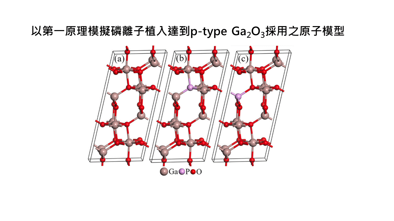
Future Tech | Electronics & OptoelectronicsTechnology Introduction: Phosphorus ion implantation into undoped Ga₂O₃ grown by MOCVD, followed by optimized annealing, yields p-type conductivity confirmed by Hall measurements. An n-type Ga₂O₃ layer is then epitaxially regrown, enabling fabrication of a lateral PN homojunction diode. These results confirm that phosphorus implantation is a reliable method for forming stable p-type Ga₂O₃, offering a viable path for future oxide semiconductor device applications. Industry Applicability: Over the past two years, our first-principles simulations identified phosphorus as a viable dopant for p-type Ga₂O₃. We found that phosphorus-related defect formation energies are low, prompting experimental studies using ion implantation. The successful formation of p-type Ga₂O₃ was confirmed and published in Materials Today Advances (2023). Device-level validation, including in-situ doping and various structures, confirms that stable, high-quality p-Ga₂O₃ is achievable.
Future Tech | Electronics & OptoelectronicsComing soon!