β-Ga2O3 Epitaxial wafers and Substrates (Novel Crystal Technology, Inc)
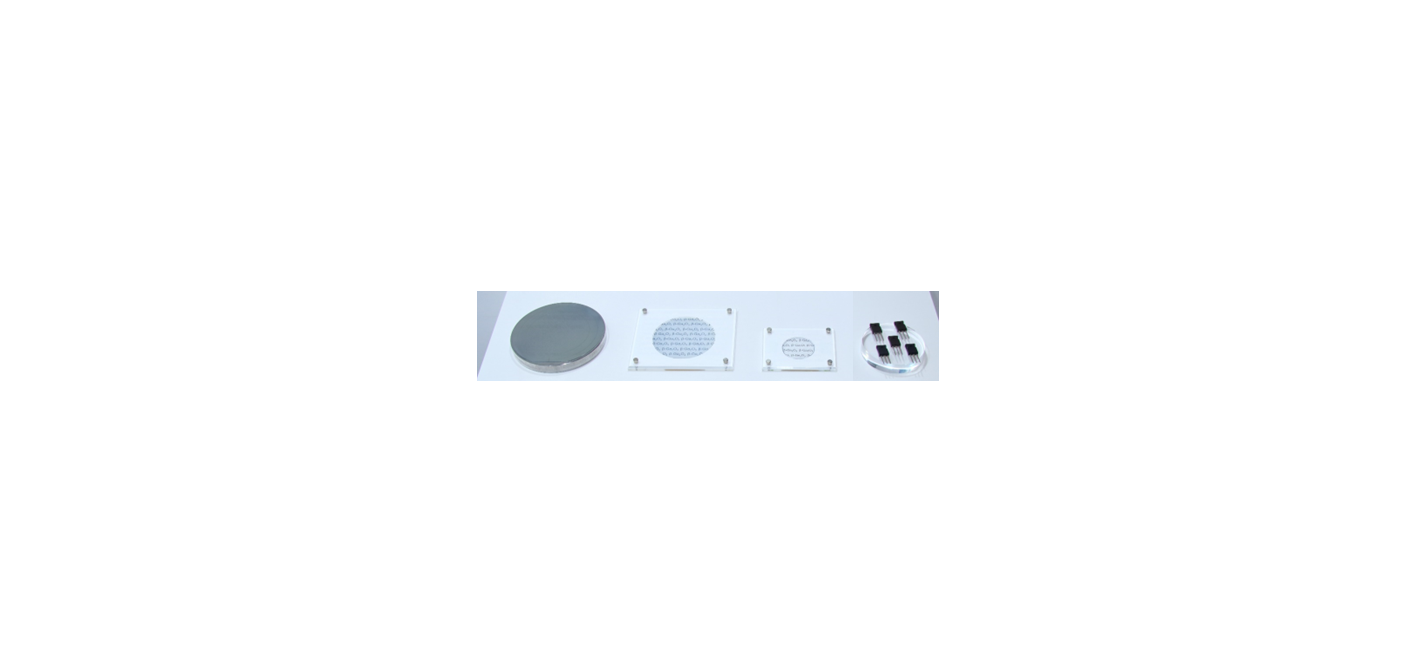
Regarding β-Ga2O3 epi-wafers and substrates for power devices, Novel Crystal Technology, Inc. is the only one manufacturer in the world. Our company possesses the following technologies.
1. Production of large, high-quality β-Ga2O3 single-crystal substrates.
2. Growth of high-purity β-Ga2O3 epitaxial layers.
3. Fabrication of β-Ga2O3 power devices (SBDs, FETs).
β-Ga2O3 has a large band-gap energy, and it can be grown from a melt source. As a result, large, high-quality single-crystal substrates can be manufactured at low cost. These characteristics make β-Ga2O3 a promising material for next-generation power electronics. In fact, β-Ga2O3 is potentially superior to GaN and SiC for power device applications.
Information &Communications, Electronics & Optoelectronics, Materials & Chemical Engineering & Nanotech, Medical care, Advanced Manufacturing & System ,Energy & Environmental Protection
Name:Shutaro Nambu
Phone:+81-75-681-7825
Address:102 Kujo CID Bldg. 13 Higashikujo-shimotonodacho, Minami-ku, Kyoto 601-8047 JAPAN
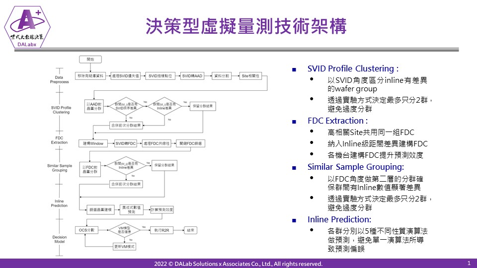
Optimizing Advanced Process Control Decision and Virtual Metrology Technology for Nano Technology Nodes for Semiconductor Manufacturing
Highly Efficient Fabrication and Applications of Bioinspired Flexible Photonic Crystals by Trapping of Structural Coloration
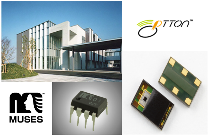
①The potential of Fukuoka Prefecture’s semiconductor industry ②High Quality Audio Device Series MUSES ③Optical Touchless Sensor"
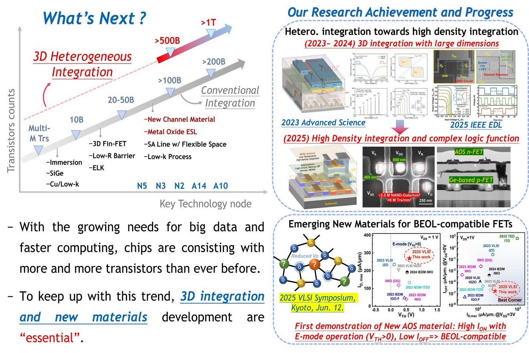
Monolithic 3D Heterogeneous Device Integration and Innovative Materials for Breaking Logic Density Limits: A Key Technology Platform for High-Density AI Computing Chips
Technology maturity:Trial production
Exhibiting purpose:Product promotion
Trading preferences:Negotiate by self
*Organization
*Name
*Phone
*Main Purpose
*Discuss Further
*Job Category
*Overall Rating
*Favorite Area
*Key Tech Focus
*Willing to Receive Updates?
Other Suggestions
Coming soon!