Highly stacked channels with extremely high-k gate stacks; Stacked nano sheet FeFET; IGZO GAA nanosheet
Highly stacked channels with extremely high-k gate stacks:
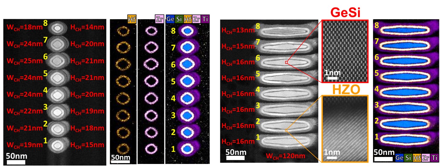
Our team has successfully integrated the extremely high-k Hf0.2Zr0.8O2 g
ate stacks (k=47) into both the 8 stacked Ge0.95Si0.05 nanowires and nan
osheets. The nanowires and nanosheets achieve the record ION per footpr
int of 9200μA/μm and the record ION per stack of 360μA at VOV=VDS=0.
5V, respectively, among all Si/GeSi/Ge 3D nFETs. The simulation of vs [Zr] i
n HZO confirms that the k can be peaked at [Zr]=80%. The significant gate
delay improvement by combining the extremely high-k gate stacks and th
e large floor number is confirmed by simulation.
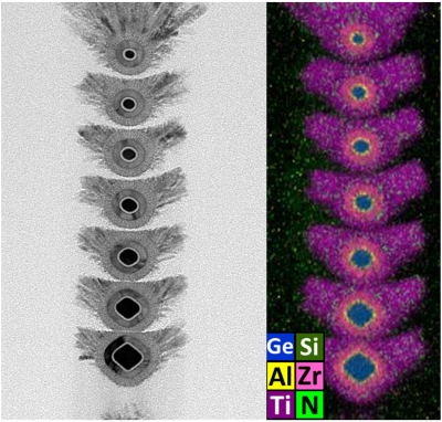
Stacked GeSi GAA Nanosheet FeFETs:
FeFETs are promising candidates for embedded non-volatile memory due
to the CMOS-compatible process for scalability, simple 1T architecture, lo
w write energy, and nondestructive read. A large memory window (MW) is
required for FeFET operations, particularly for multi bits. Our team has suc
cessfully developed the world first stacked GeSi nanosheet gate-all-aroun
d (GAA) FeFETs, featuring large memory window of 1.8V at the low write v
oltage of 2V, the stable storage with data retention of >1E4 seconds, high
endurance >1E11 cycles, CMOS compatible process, and low thermal bud
get of 400oC.
Amorphous InGaZnO (a-IGZO) Gate-all-around (GAA) Nanosheet FET:
A-IGZO has been received much attention recently due to its low process t
emperature, high electron mobility, and high uniformity, especially on the
monolithic applications. Despite a-IGZO features extremely low leakage c
urrent, the moderate mobility is still not compatible to the traditional gro
up IV materials. GAA structure can not only increase the Ion but also decre
ases the subthreshold swing (SS) and leakage current. Our team has succe
ssfully developed the world first a-IGZO GAA nanosheet FET, featuring ne
arly ideal SS of 61 mV/dec, extremely low Ioff of <1E-7 uA/um, high Ion/Io
ff of >1.3E8、low DIBL of 44mV/V, positive threshold voltage and CMOS c
ompatible process
At present, the University consists of 16 colleges, 58 departments, 146 graduate institutes, as well as 34 Master's and PhD degree programs. NTU's programs cover a wide array of disciplines across science, arts, and the humanities, with up to 8,000 courses made available for selection each semester.
High mobility materials, process, stacked channels, and thermal circuit simulation; Ferroelectric X:HfO2 for Negative Capacitance and POC(Proof-of-Concept) Applications; Atomic layer technologies for
Hybrid CMOS Inverter Comprised of Thin Film Transistors with Hetero-channel for Monolithic 3D-ICs and Ultra-high Resolution Flat-Panel Displays Applications
Resonant Magnetic Coupling Wireless Power Transfer System with Calibration Capabilities of Its Inductor-Capacitor Resonant Frequencies
Dual M-Layers Avalanche Photodiodes with High Single-Photon Detection Efficiency and High Saturation Output Power for Lidar applications
Technology maturity:Experiment stage
Exhibiting purpose:Display of scientific results
Trading preferences:Negotiate by self
*Organization
*Name
*Phone
*Main Purpose
*Discuss Further
*Job Category
*Overall Rating
*Favorite Area
*Key Tech Focus
*Willing to Receive Updates?
Other Suggestions
Coming soon!