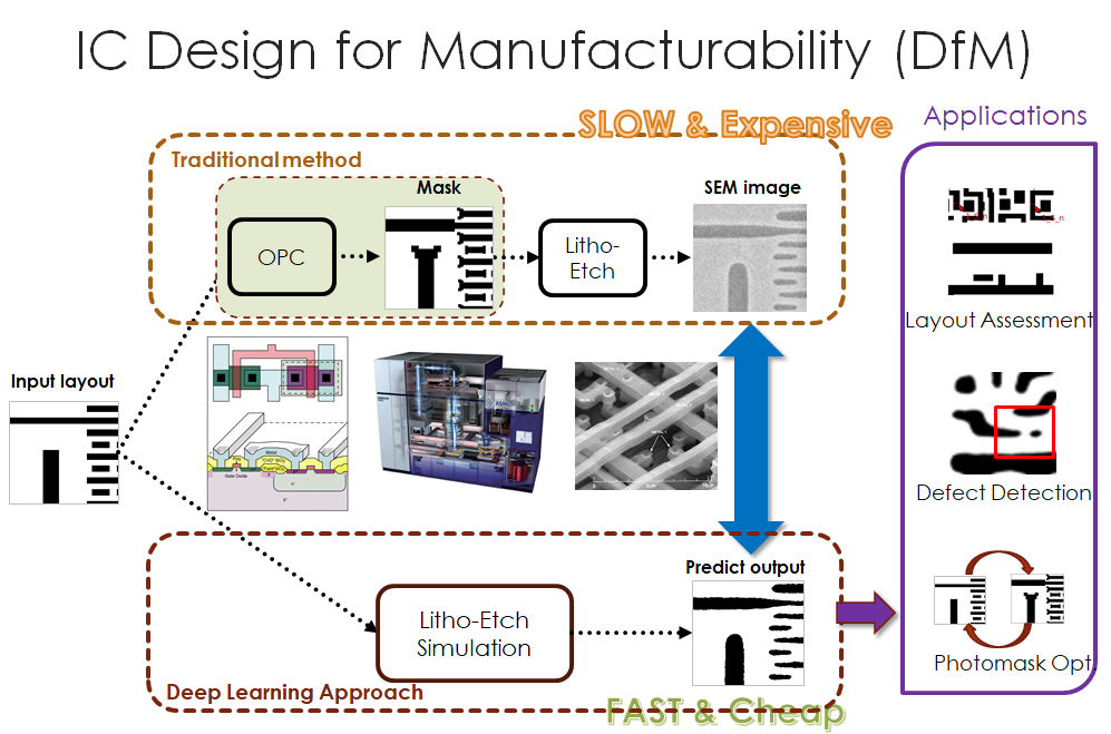
We exploit deep learning techniques to develop EDA tools for semiconductor manufacturing. Our EDA tools can predict circuit shape distortions caused by the lithography processes and thus assess the photomask correction results at an early stage. These tools can be applied to layout's OPC simulation, layout hotspot detection, IC defect detection, and photomask optimization.
National Chung Hsing University (NCHU), established in 1919, is located in Taichung, Taiwan. It is a comprehensive university offering a wide range of programs in agriculture, engineering, science, humanities, and social sciences. NCHU is known for its strong emphasis on research, innovation, and sustainability. With a focus on international collaboration and community engagement, the university strives to cultivate leaders with global perspectives. NCHU aims to contribute to society through high-quality education, advanced research, and fostering a diverse academic environment.
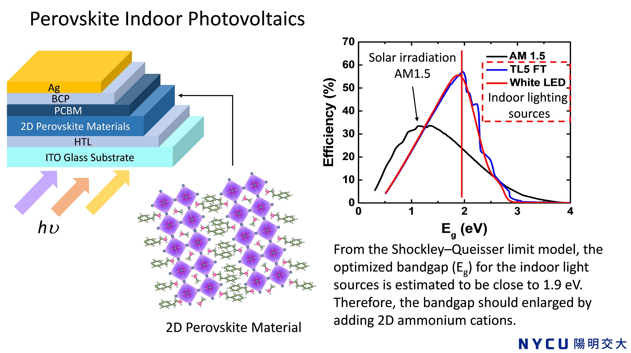
Emerging Two-Dimensional Perovskite Indoor Photovoltaics for Children Healthcare System Based on Internet of Things Technologies
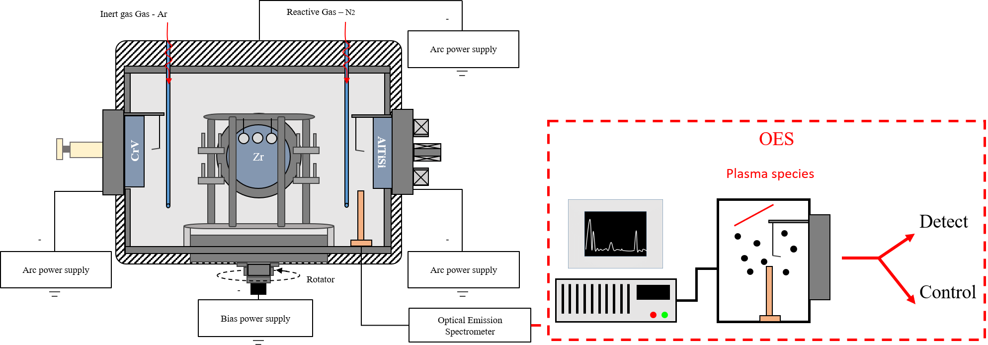
High Entropy Alloy Nitride Hard Coatings Prepared by Cathodic Arc Deposition and Their Applications of Micro End Mills
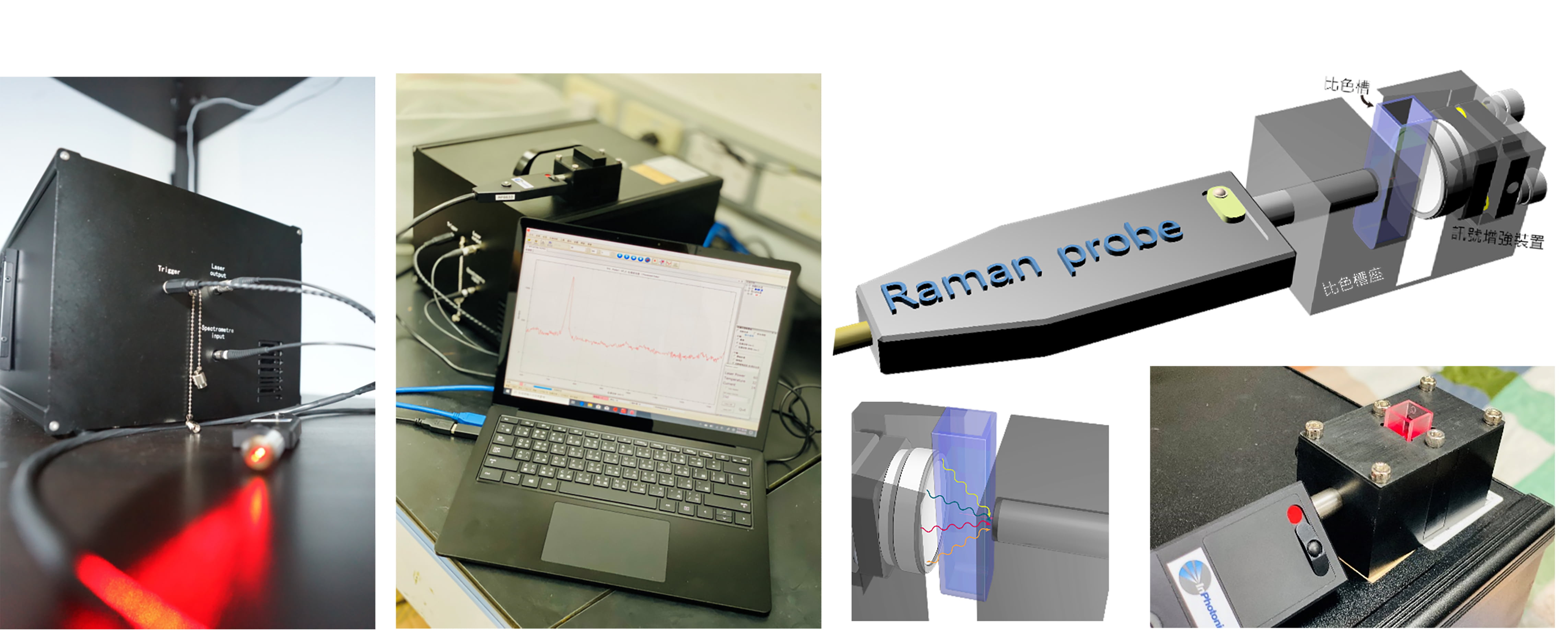
Magnetic and 2D metallic Nanoparticle Arrays of Surface-Enhanced Raman Spectroscopy (SERS) Detection Platform for Environmental-Biomedical Sensing
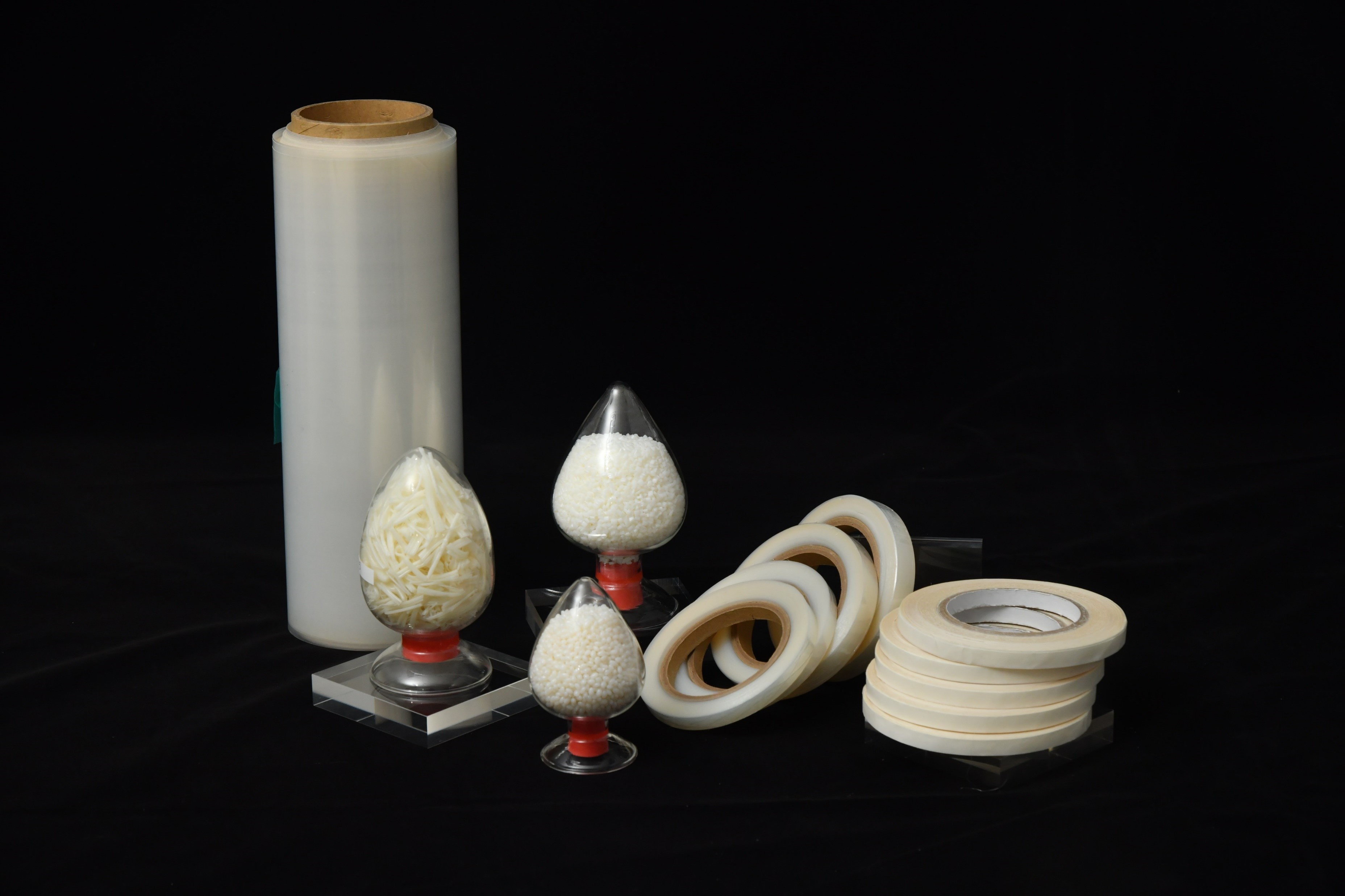
TEXBONDER® Bonding Instead of Sewing for Single-Material Garments – Improving Recyclability and Circularity
Technology maturity:Experiment stage
Exhibiting purpose:Display of scientific results
Trading preferences:Negotiate by self
*Organization
*Name
*Phone
*Main Purpose
*Discuss Further
*Job Category
*Overall Rating
*Favorite Area
*Key Tech Focus
*Willing to Receive Updates?
Other Suggestions
Coming soon!