Low Temperature Atomic Layer Deposition Technology with High Aspect Ratio Multi-component
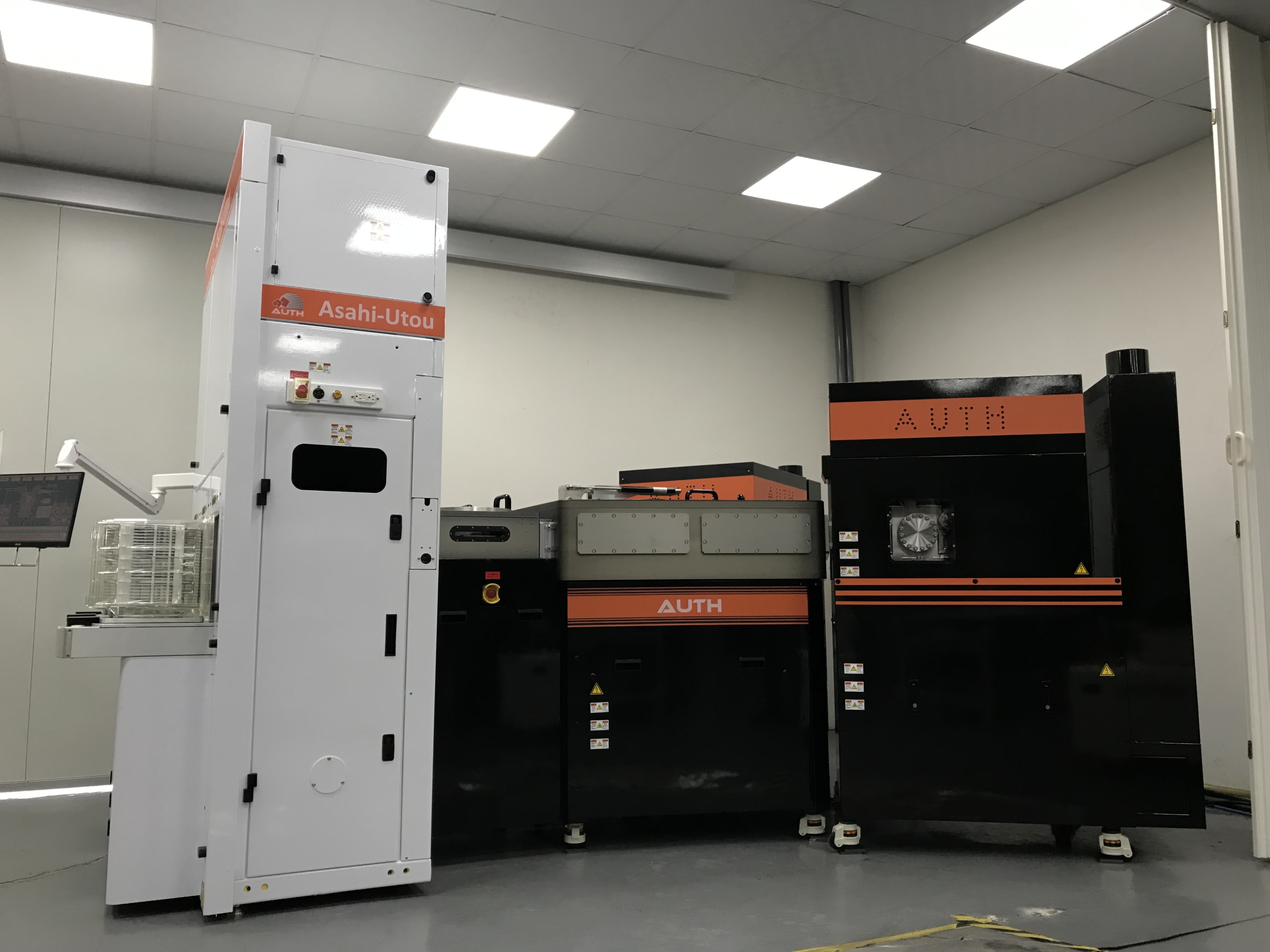
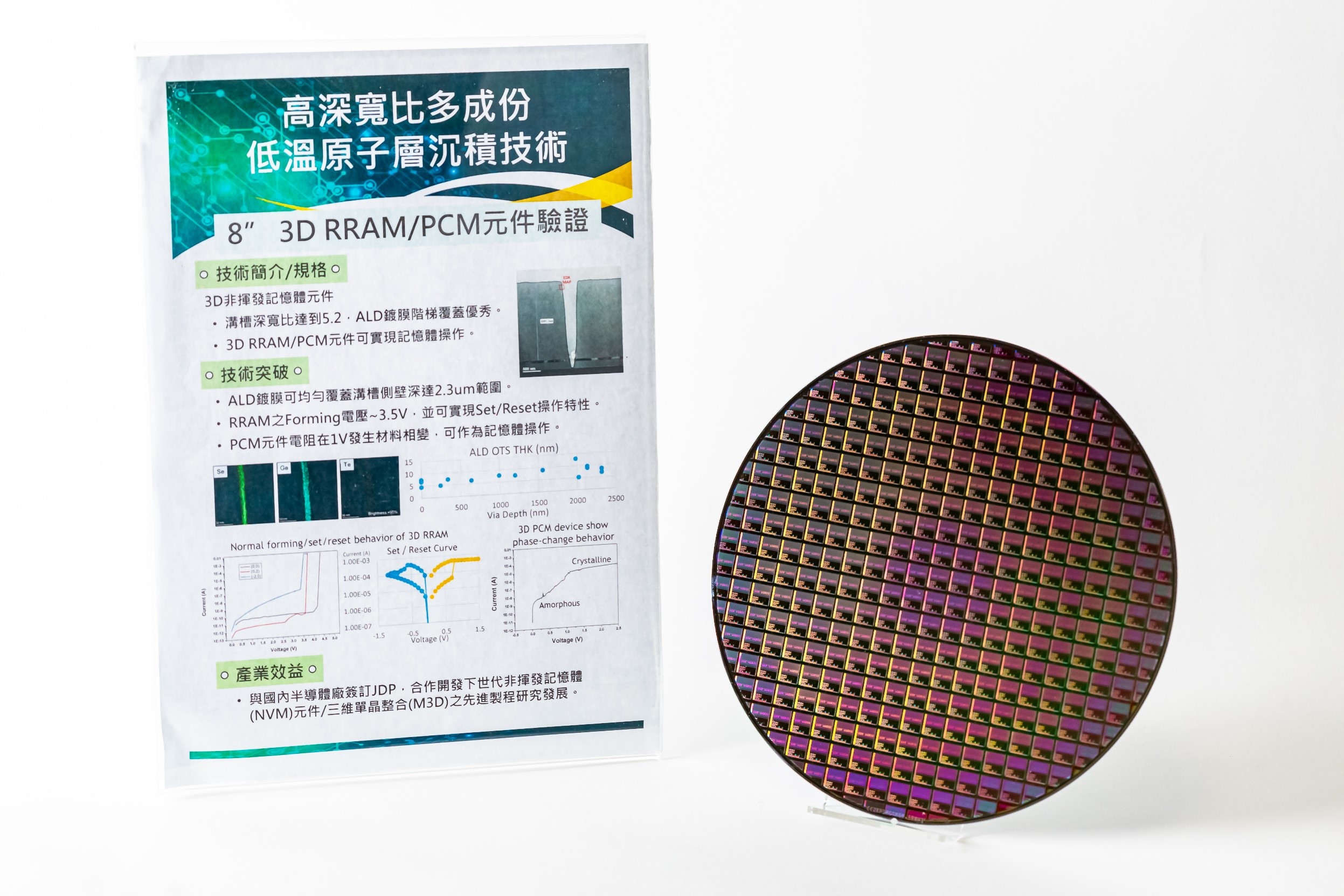
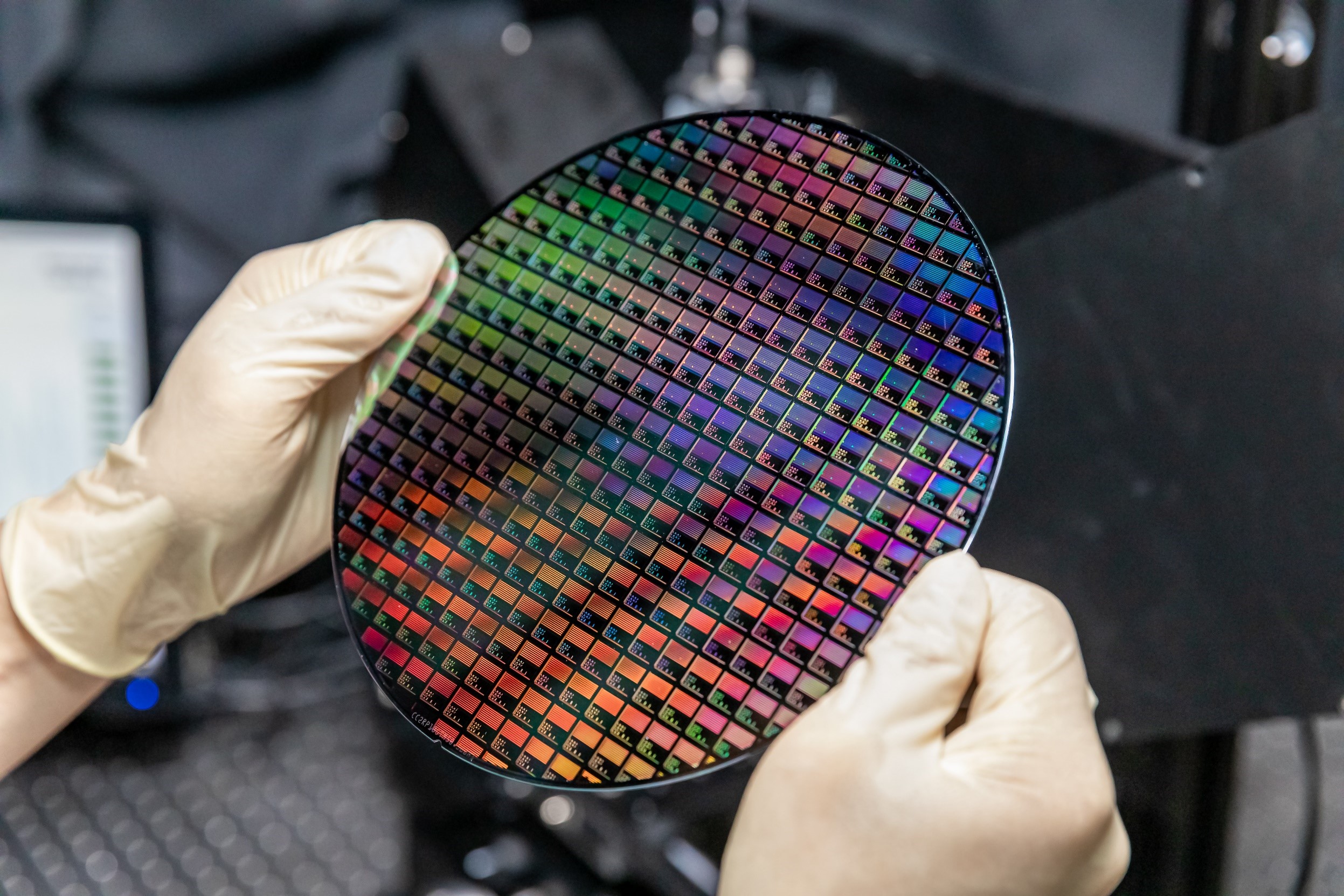
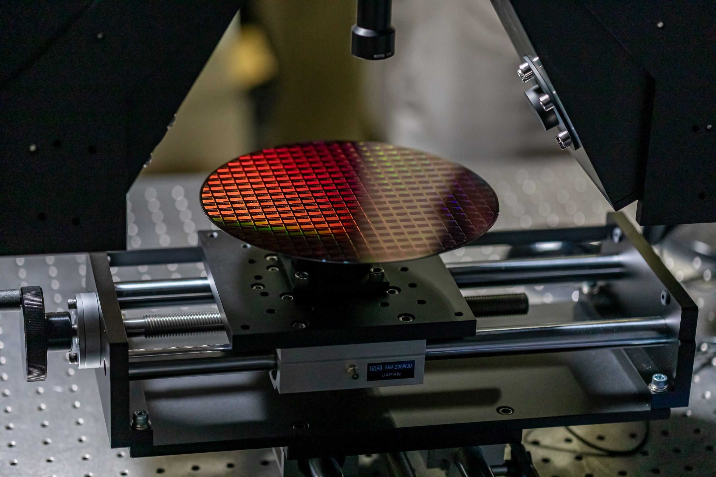

Nowadays PVD and PECVD equipment cannot meet the requirements for multi-component thin film deposition of 3D structural devices with an aspect ratio more than 10, which poses a great challenge to the next-generation semiconductor manufacturing process. The bidirectional flow with composite discrete pulse feed-in methods of multi-component atomic layer deposition is the first to break through the limitation that precursors are difficult to penetrate into pores, and to achieve uniform conformal coverage on the surface and bottom layers of 3D structures. And it achieves high aspect ratio multi-component conformal three-dimensional structure coverage nano film deposition. We also developed an anti-vibration phase modulation spectroscopic ellipsometer, which uses multiple discrete wavelengths for simultaneous measurement. It reduces noise and obtains a high signal-to-noise (SN) ratio by using phase locked-in detection. The film thickness measurement discrimination rate is ≤1nm, achieving high speed (sampling speed ~10 kHz) anti-vibration real-time film thickness measurement. We also successfully developed a multi-cell 3D memory multi-component device manufacturing process and verification. The difficulties of integrating semiconductor process are also overcome. This technology can be applied to high-speed and low-power memory processes required by the next-generation IC industry. It can not only replace imports, but also break the current monopoly on imports of front-end equipment and increase domestic market share. Domestic and foreign patents have been certified, breaking through the international patent technology blockade, and won the 2023 R&D 100 Award Winner and the ITRI’s Outstanding Research Award. The technology will be transferred to domestic equipment manufacturers for them to co-produce, and will be brought into semiconductor manufacturing plants for the future application. Therefore, the capability of localizing the equipment development will be improved.
ITRI is a world-leading applied technology research institute with more than 6,000 outstanding employees. Its mission is to drive industrial development, create economic value, and enhance social well-being through technology R&D. Founded in 1973, it pioneered in IC development and started to nurture new tech ventures and deliver its R&D results to industries. ITRI has set up and incubated companies such as TSMC, UMC, Taiwan Mask Corp., Epistar Corp., Mirle Automation Corp., and Taiwan Biomaterial Co.
Name:
Phone:
Address:195, Sec. 4, Chung Hsing Rd., Chutung, Hsinchu, Taiwan 31040, R.O.C.
I790028
Advanced Automatic Detection Technology for EL Inspection and IR Ther mal Defects in Solar Modules
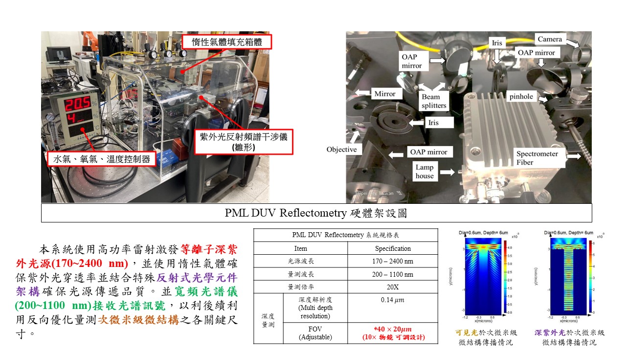
Optical critical-dimension measuring technology for high-aspect-ratio microstructures in advanced semiconductor packaging
Low-Temperature Defects Elimination Technology for Semiconductor devices
Low Temperature Polycrystalline Silicon Oxide (LTPO) TFT Architecture with Memory-embedded in Pixel for High-resolution and Power-saving Near-eye VR/AR Displays Applications
Technology maturity:Experiment stage
Exhibiting purpose:Technology transactions、Patent transactions、Product promotion、Display of scientific results
Trading preferences:Technical license/cooperation、New products development、Negotiate by self、Non-exclusive license、Exclusive license/assignment
Coming soon!