The Future of 2D Materials: Transistors, Transparent Electrodes and Photodetectors
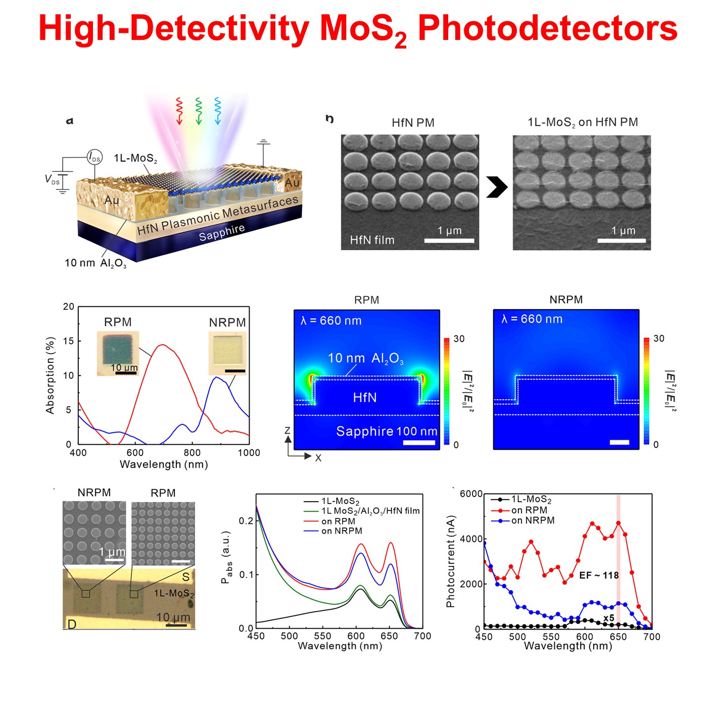
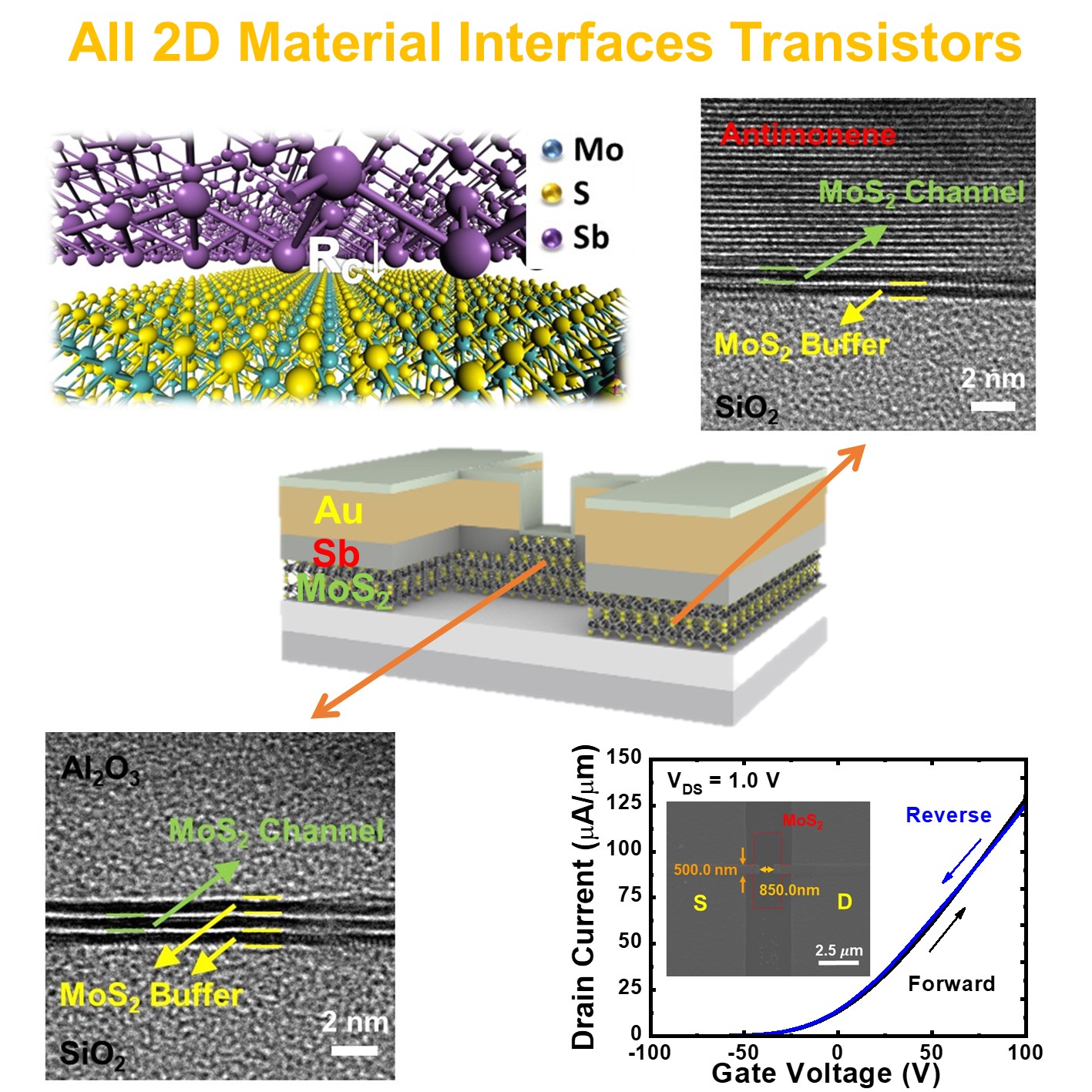


Conductive 2D materials as low-contact-resistance electrodes → MoS2(下標) transistors with all 2D material interfaces.
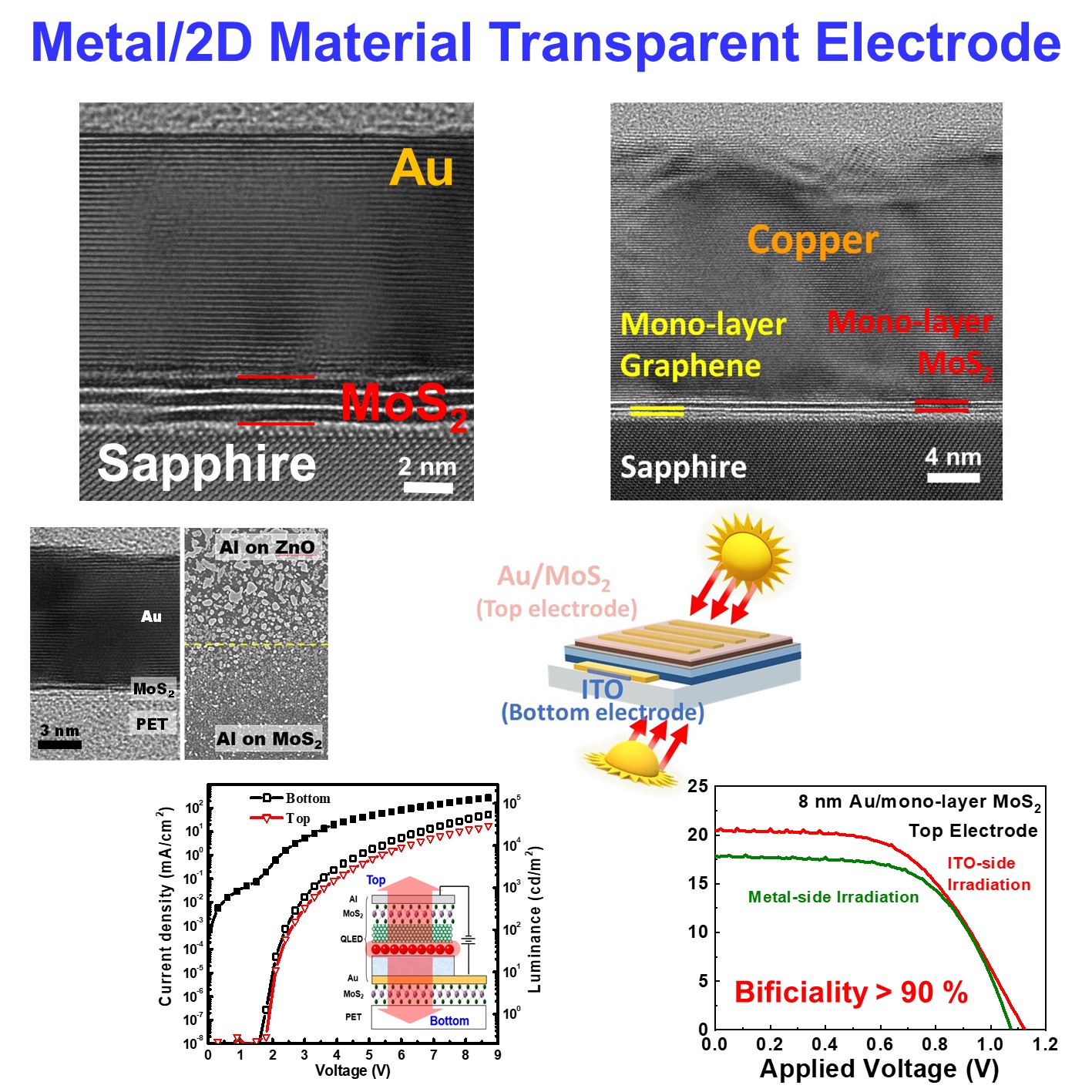
van der Waals epitaxy of 2D materials → quantum-dot light-emitting diodes and bifacial solar cells with thin metal/2D material transparent electrodes.
Resonant plasmonic nanostructures → ultrathin phototransistors with ultrahigh responsivity
Wafer-scale and multi-layer 2D materials → photovoltaic vertical devices and photoconductive planar photodetectors with shortened response times
Founded in 1928, Academia Sinica has earned a reputation for being Taiwan’s national academic institution. Our statutory mission is to pursue research excellence, nurture academic talent, and issue policy advisories. Academia Sinica currently has 24 institutes and 9 research centers located in three research sections: the Mathematics and Physical Sciences Division, Life Sciences Division, and Division of Humanities and Social Sciences. There are currently over 8,000 research fellows, research technicians, assistants, and administrative staff, making it a rare research institution internationally that achieves a balanced development in both natural sciences and humanities and social sciences.
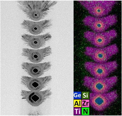
High mobility materials, process, stacked channels, and thermal circuit simulation; Ferroelectric X:HfO2 for Negative Capacitance and POC(Proof-of-Concept) Applications; Atomic layer technologies for
Hybrid CMOS Inverter Comprised of Thin Film Transistors with Hetero-channel for Monolithic 3D-ICs and Ultra-high Resolution Flat-Panel Displays Applications
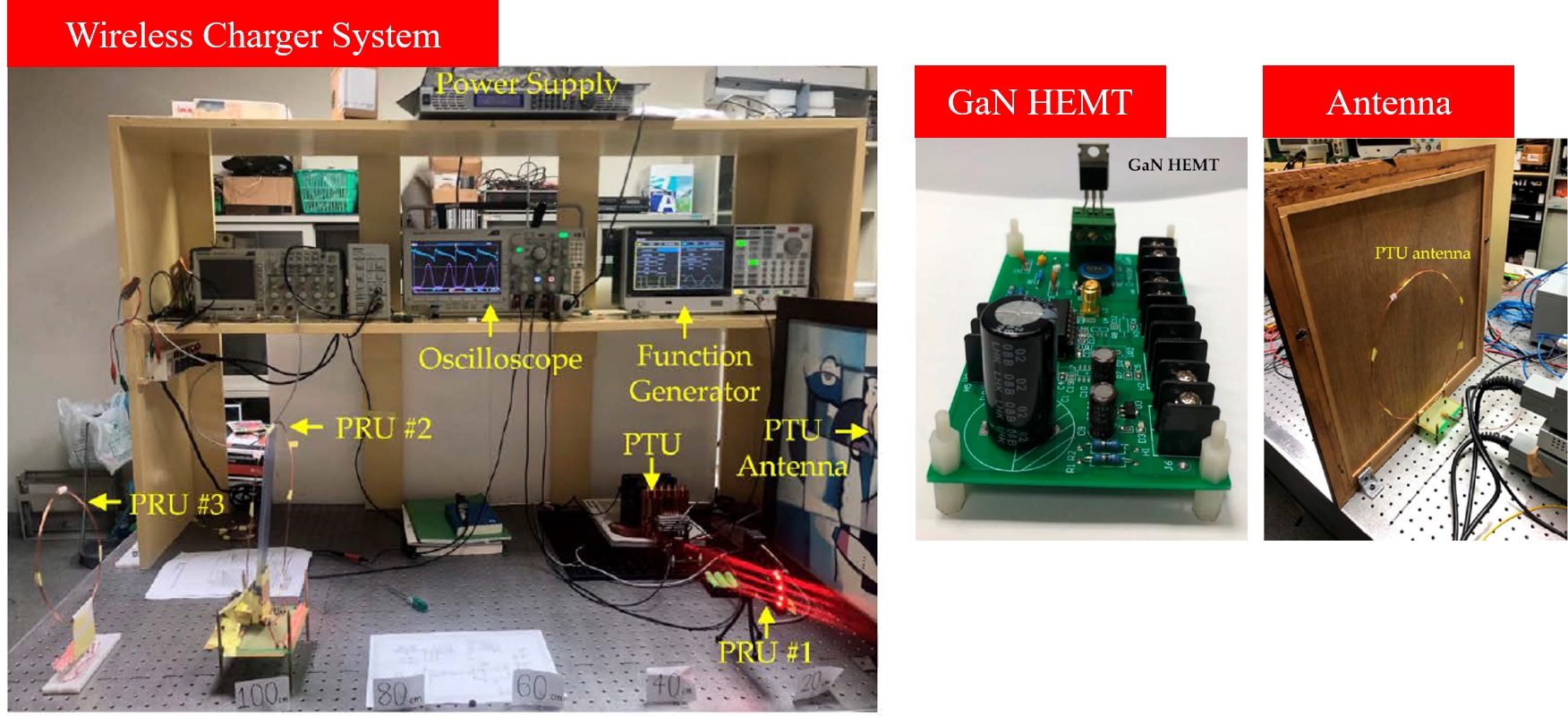
The novel technology of high efficiency GaN transistors for high frequency and high power application.
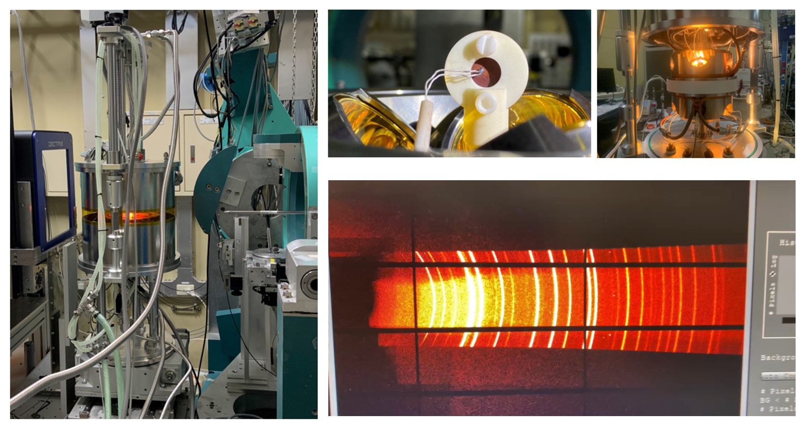
Refining area at 1600°C: Advanced synchrotron X-ray views into the black box of blast furnaces, understands ironmaking process, and illuminates the bright road to net-zero carbon emissions
Technology maturity:Prototype
Exhibiting purpose:Display of scientific results
Trading preferences:Negotiate by self
*Organization
*Name
*Phone
*Main Purpose
*Discuss Further
*Job Category
*Overall Rating
*Favorite Area
*Key Tech Focus
*Willing to Receive Updates?
Other Suggestions
Coming soon!