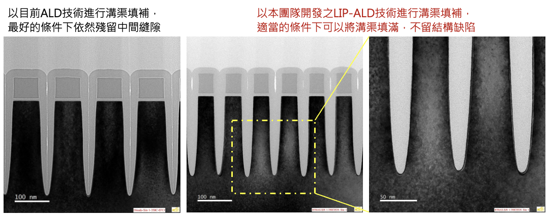
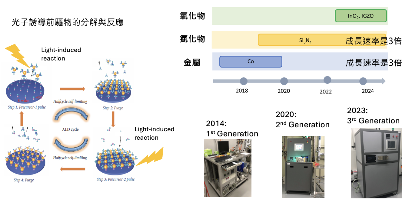


Existing ALD techniques fail to address the issues of residual voids and seam defects in trench filling. We have developed a photo-induced precise ALD (LIP-ALD) technique over the past decade, which enables precise control of atomic deposition for gap fills. It has achieved seamless, pore-free, and low-impurity dielectric material deposition in high aspect ratio N3 and N2 node structural wafers. AMAT, AL, and TSMC have co-joined the research of this novel LIP-ALD process in NTHU with our team.
National Tsing Hua University (NTHU), established in 1911 and located in Hsinchu, Taiwan, is one of the top research universities in the country. NTHU offers a wide range of programs in fields such as engineering, science, management, and humanities. The university is known for its strong emphasis on innovation, research excellence, and fostering global perspectives. With a commitment to academic rigor and interdisciplinary collaboration, NTHU plays a key role in advancing knowledge and technological development, contributing to both Taiwan’s growth and the global academic community.

The Intelligent Cloud Platform for the Machinery Industry and on-premise Taiwan Machinery Standard Runtime networking technologies.
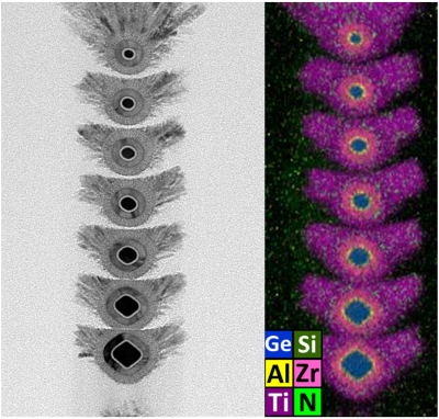
High mobility materials, process, stacked channels, and thermal circuit simulation; Ferroelectric X:HfO2 for Negative Capacitance and POC(Proof-of-Concept) Applications; Atomic layer technologies for
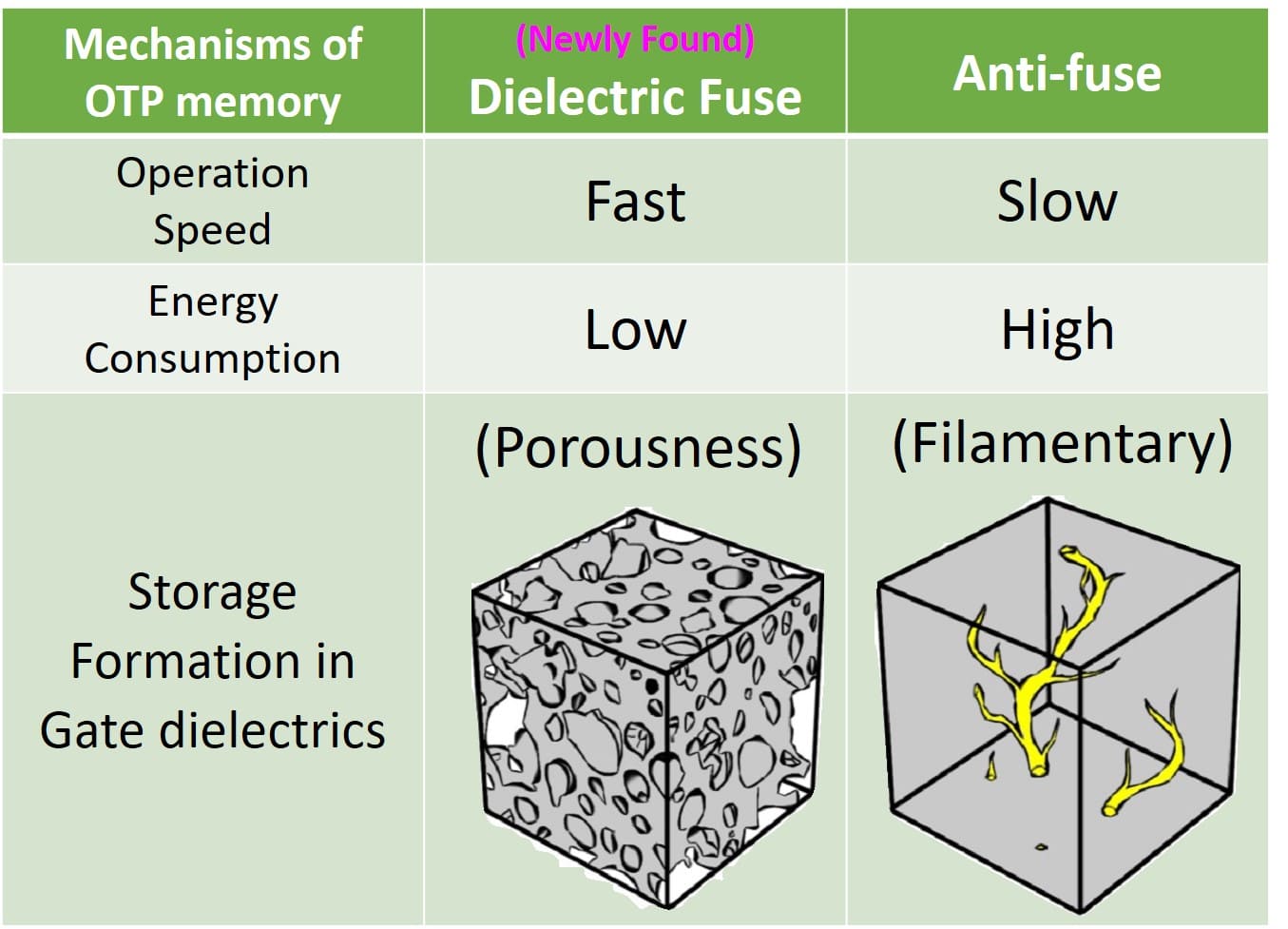
A Low-cost, Low-power, and High-speed “Dielectric-fuse Breakdown OTP” (dFuse OTP) Fully Integrated on CMOS Platform without Additional Masks
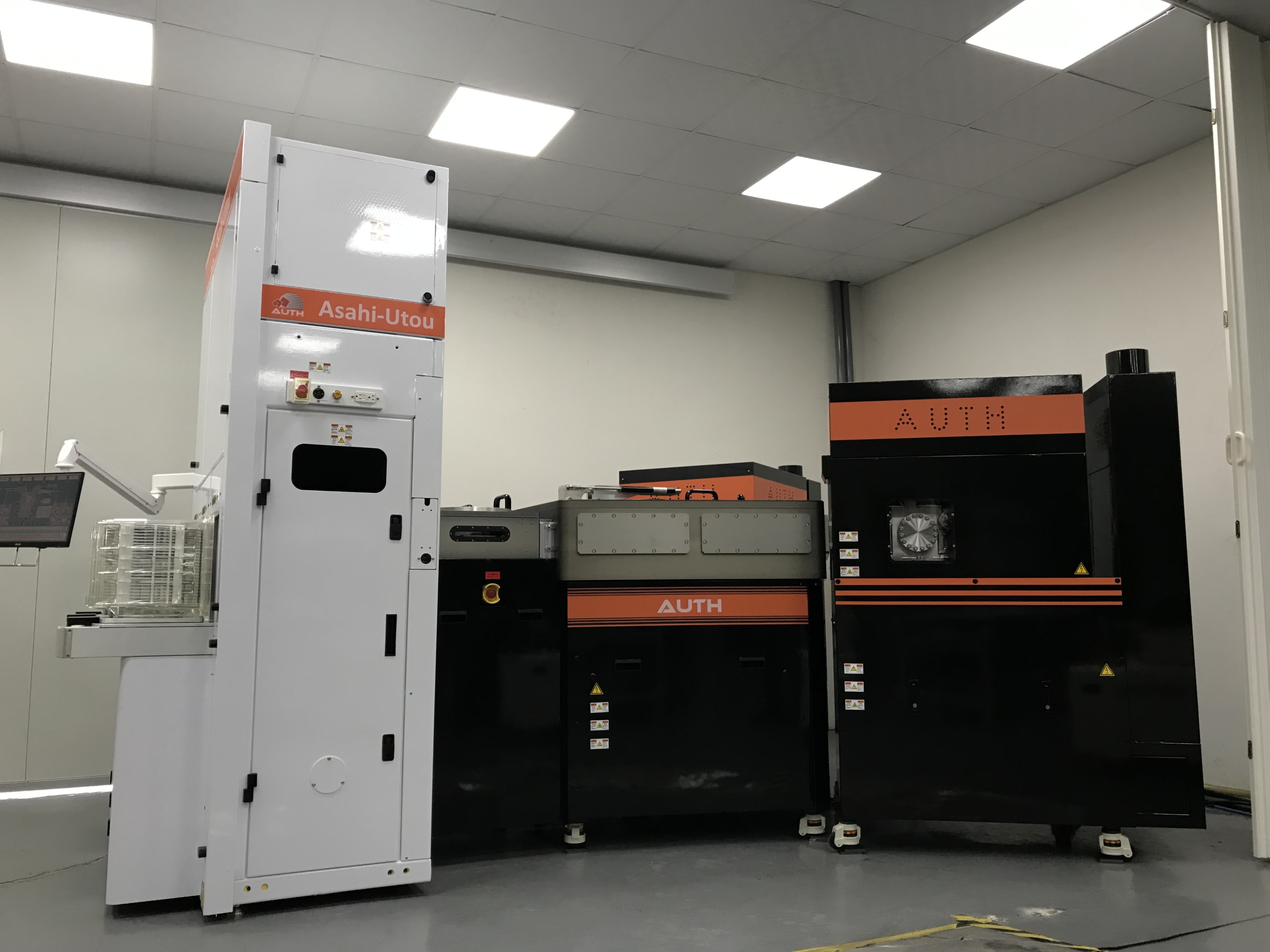
Low Temperature Atomic Layer Deposition Technology with High Aspect Ratio Multi-component
Technology maturity:Prototype
Exhibiting purpose:Display of scientific results
Trading preferences:Negotiate by self
*Organization
*Name
*Phone
*Main Purpose
*Discuss Further
*Job Category
*Overall Rating
*Favorite Area
*Key Tech Focus
*Willing to Receive Updates?
Other Suggestions
Coming soon!