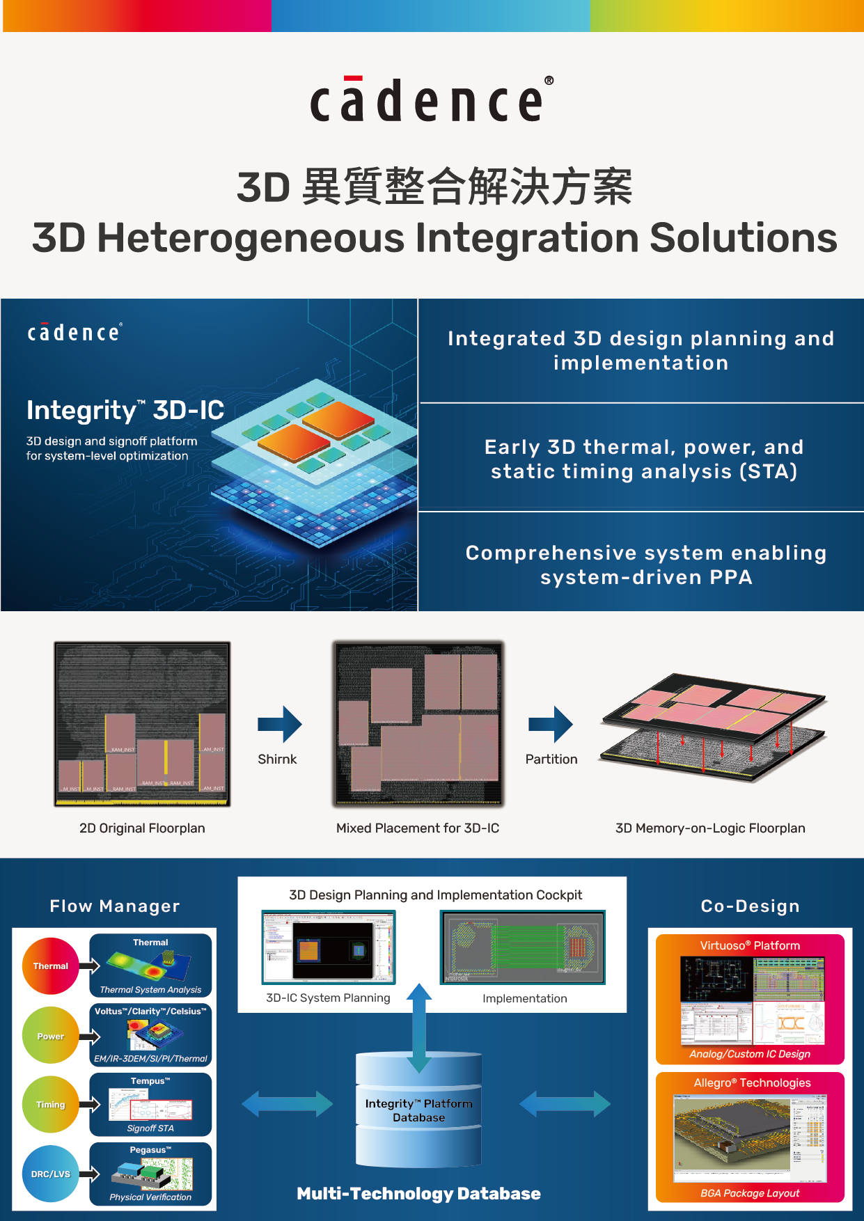

The Cadence® Integrity™ 3D-IC Platform is a high-capacity, unified design and analysis platform for designing multiple chiplets. Built on the infrastructure of Cadence’s leading digital implementation solution, the Innovus™ Implementation System, the platform allows system-level designers to plan, implement, and analyze any type of stacked die system for a variety of packaging styles (2.5D or 3D). Integrity 3D-IC is the industry’s first integrated system- and SoC-level solution that enables system analysis, including co-design, with Cadence’s Virtuoso® and Allegro® analog and package implementation environments.
Cadence成立於1988年,在運算軟體領域擁有超過30年的經驗,是當今電子設計的領導者。公司以智慧系統設計(Intelligent System Design)為核心策略,提供軟體、硬體及半導體IP,協助電子設計從概念走向應用實現。Cadence服務全球客戶,從晶片、印刷電路板至整體系統打造尖端與創新的電子產品,以應用於行動、消費性電子、超大型運算、5G通訊、汽車、航太、工業及健康醫療等當今最活躍的市場。Cadence是業界唯一能提供從系統設計所涵蓋的積體電路(IC)、封裝與電路板間無縫設計全流程解決方案的電子設計自動化(EDA)公司,30多年來持續驅動半導體創新。
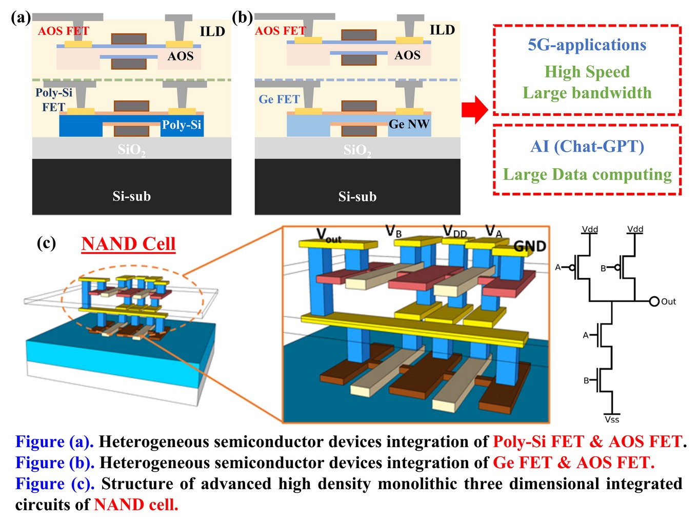
Novel Monolithic 3D Heterogeneous Semiconductor Device Integration f or Ultra-High-Density (20M NAND-Gate/mm^2) Logic Gate Circuits
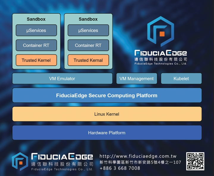
FiduciaEdge Computing Platform (fECP) – Trustworthy Heterogeneous Edge Computing Solution
A New Hardware-security Technique for 5G-AIOT Applications: A Low-cost, Low-power, and High-speed “Dielectric-fuse Breakdown OTP” (dFuse OTP) Fully Integrated on CMOS Platform without Additional Masks
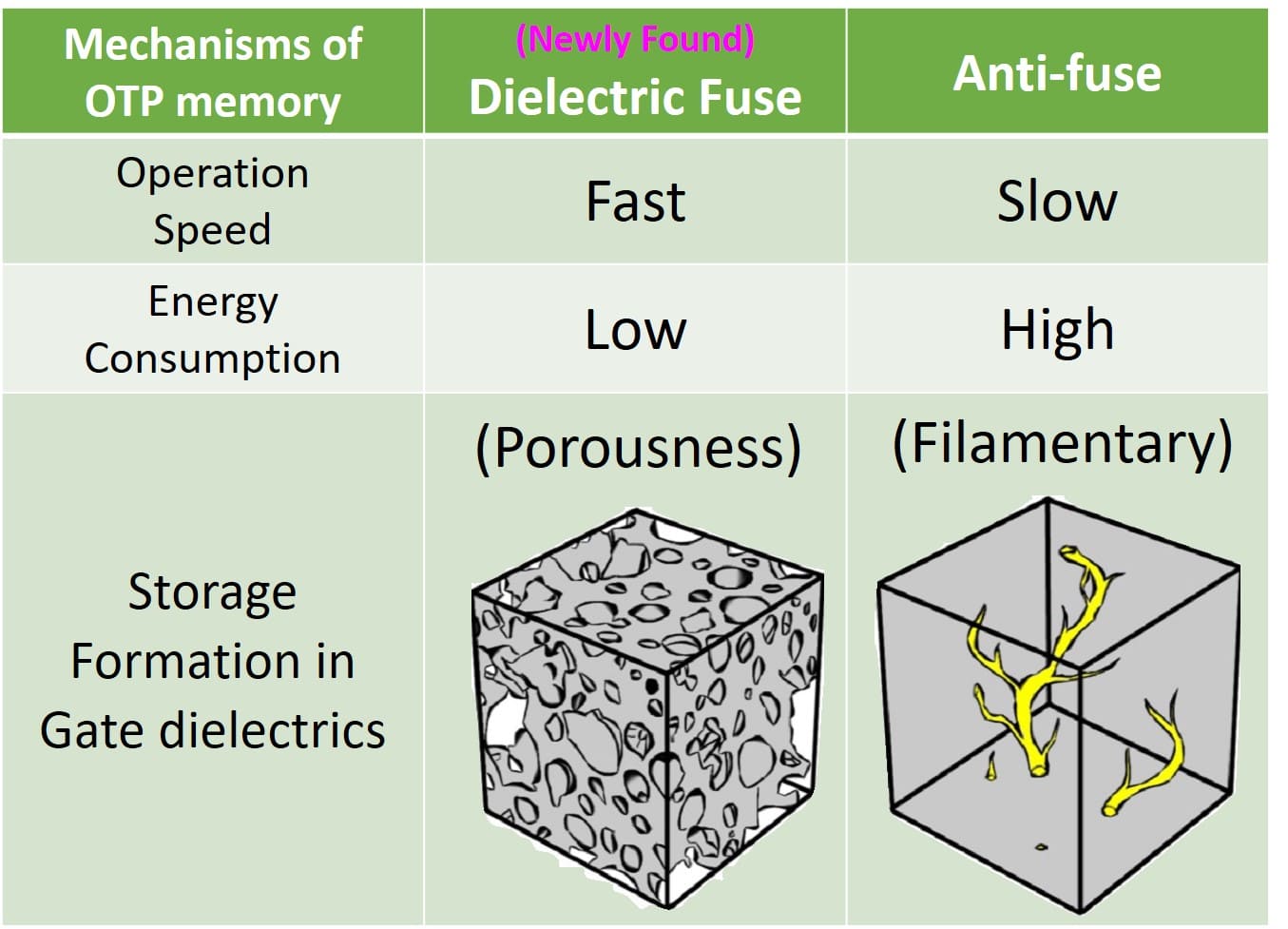
A Low-cost, Low-power, and High-speed “Dielectric-fuse Breakdown OTP” (dFuse OTP) Fully Integrated on CMOS Platform without Additional Masks
Technology maturity:Mass production
Exhibiting purpose:Display of scientific results
Trading preferences:New products development
Coming soon!