Technology Introduction:
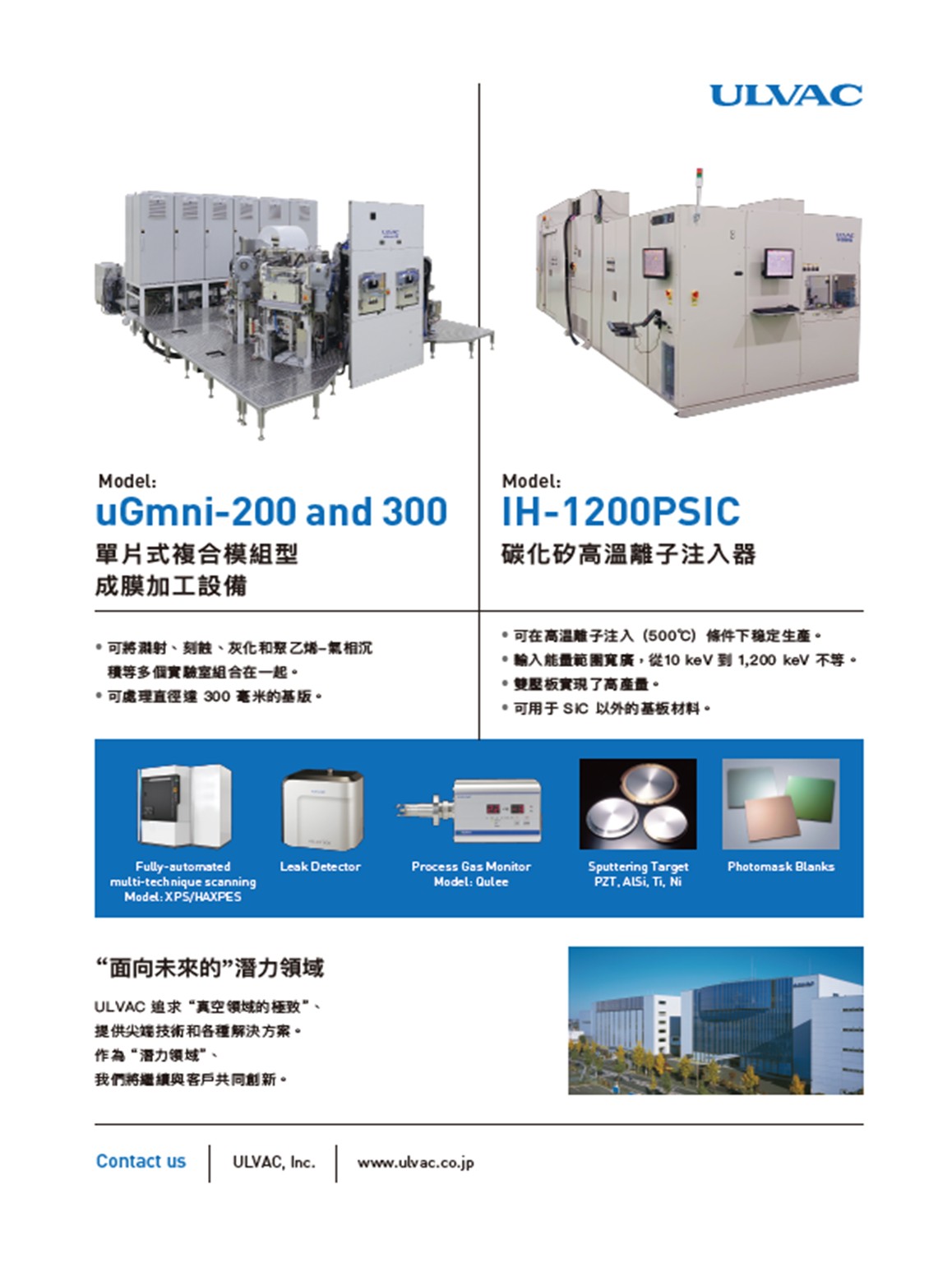
ULVAC has developed an advanced system for processing silicon carbide (SiC) materials. It enhances wafer stability, increases throughput, and reduces contamination, ensuring faster and cleaner production of high-quality SiC wafers. These wafers are ideal for high-temperature, high-frequency, and high-voltage applications, including EV chargers, industrial motors, and renewable energy systems.
Industry Applicability:
ULVAC’s high-energy ion implantation equipment for compound semiconductors is designed for industries needing advanced materials for high-performance devices. It supports mass production and prototyping, enabling devices with higher efficiency, reliability, and performance. Applications include automotive electronics, renewable energy, telecommunications, and industrial systems.
Back in 1952, ULVAC was still a fledgling venture that had just been founded by young engineers aspiring to contribute to industrial and scientific advancement through the use of vacuum technologies with the financial support of six angel investors. While continuing to cherish the entrepreneurial spirit that it has embraced since its establishment, ULVAC remains committed to creating new value by pursuing cutting-edge innovation for our vacuum technologies. To this end, our company works hand-in-hand with manufacturers in a wide range of industries to deliver products that are employed in not only liquid-crystal flat-panel displays, semiconductors, and electronic components, but also the types of machinery used in the automotive, food, pharmaceutical, and other general industries. The ULVAC Group employs a unique business approach to offer comprehensive solutions for a wide range of industries by mobilizing its rich variety of vacuum technologies. Examples of products that employ these technologies include vacuum equipment, components, materials, and analytical instruments, as well as a broad range of customer solutions. ULVAC responds to ongoing changes dynamically and harnesses the new business opportunities that they present by leveraging the group's collective strength and capacity for innovation to swiftly cater to customer needs in a variety of fields. In doing this, we aspire to act as the driving force behind industrial and scientific advancement with the aim of ushering in a flourishing future.

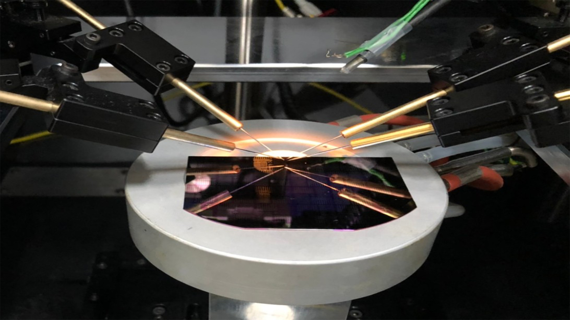
Enhancing Anodization of Semiconductor Materials Technology with Waf er Bonding Transforming Interface Function
Low Temperature Polycrystalline Silicon Oxide (LTPO) TFT Architecture with Memory-embedded in Pixel for High-resolution and Power-saving Near-eye VR/AR Displays Applications
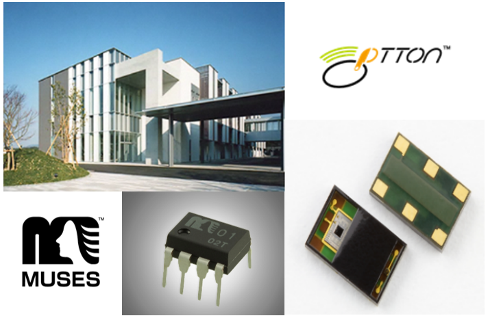
①The potential of Fukuoka Prefecture’s semiconductor industry ②High Quality Audio Device Series MUSES ③Optical Touchless Sensor"
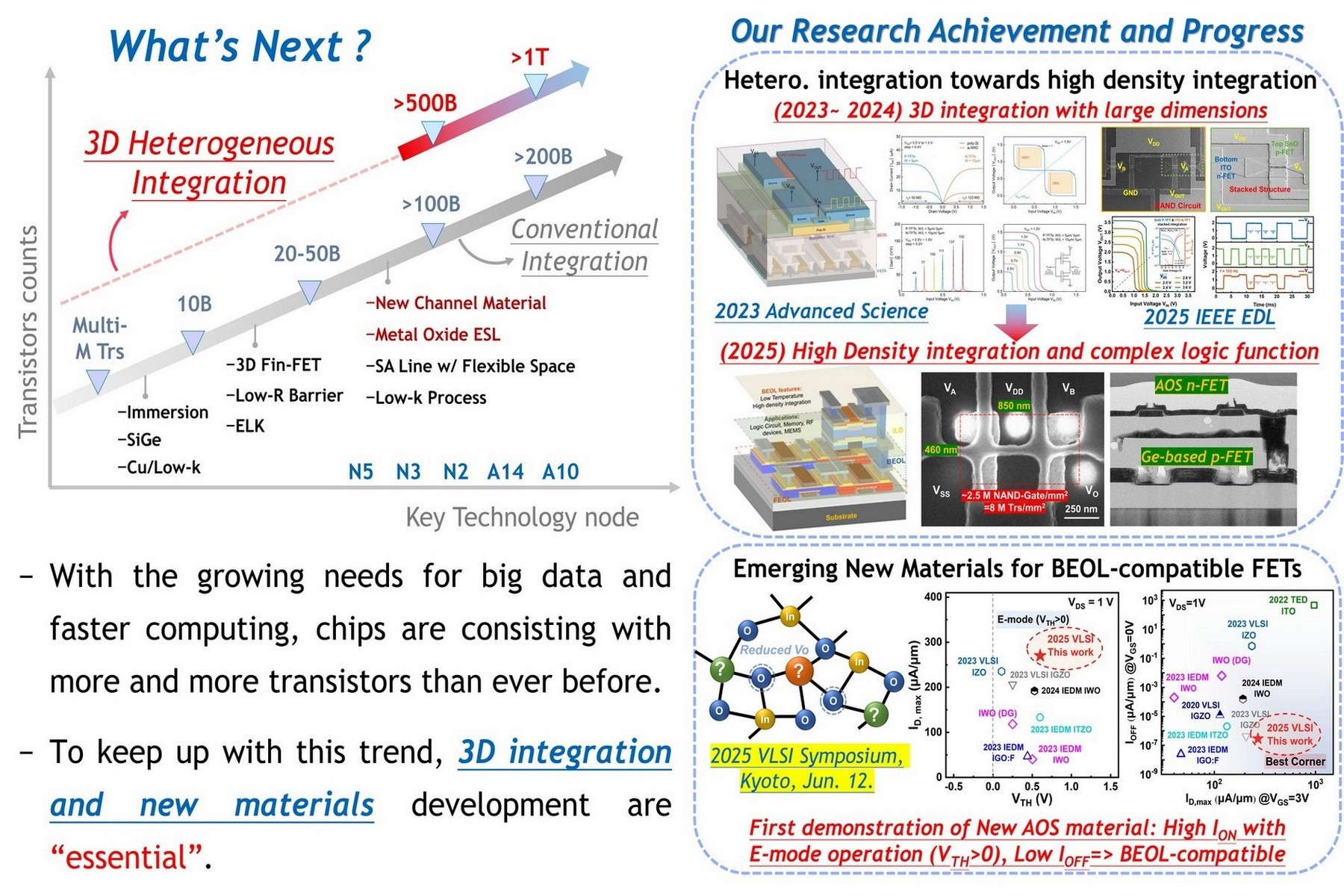
Monolithic 3D Heterogeneous Device Integration and Innovative Materials for Breaking Logic Density Limits: A Key Technology Platform for High-Density AI Computing Chips
Technology maturity:Mass production
Exhibiting purpose:Product promotion
Trading preferences:Technical license/cooperation
*Organization
*Name
*Phone
*Main Purpose
*Discuss Further
*Job Category
*Overall Rating
*Favorite Area
*Key Tech Focus
*Willing to Receive Updates?
Other Suggestions
Coming soon!