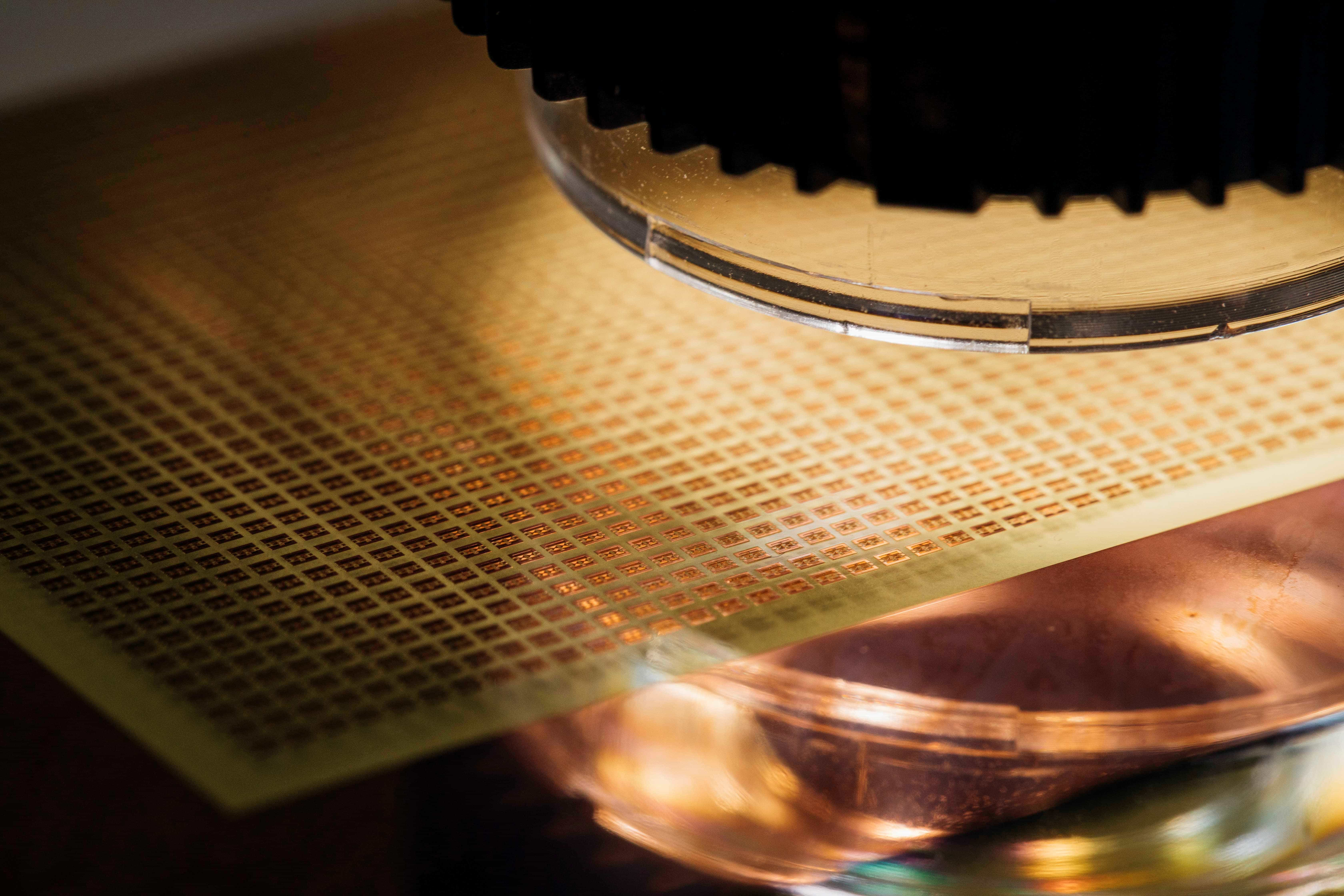
Development of In-line Wafer-level High Aspect Ratio TSV Inspection Technology

3D IC is a three-dimensional stacking and packaging process that realizes lower latency and high speed. The CMS of ITRI adopts the world’s first high aspect ratio (>30) Through Silicon Via (TSV) inspection technology, which is different from traditional optical inspection technology that can only reach the aspect ratio of 10. It solves the problem that the industry can only use destructive inspection in high aspect ratio silicon vias.
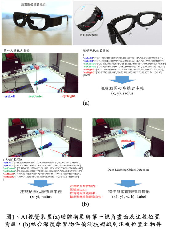
3D Printed Prosthetic Arm using Eye-Tracking and Artificial Intelligence Visual Recognition Technology
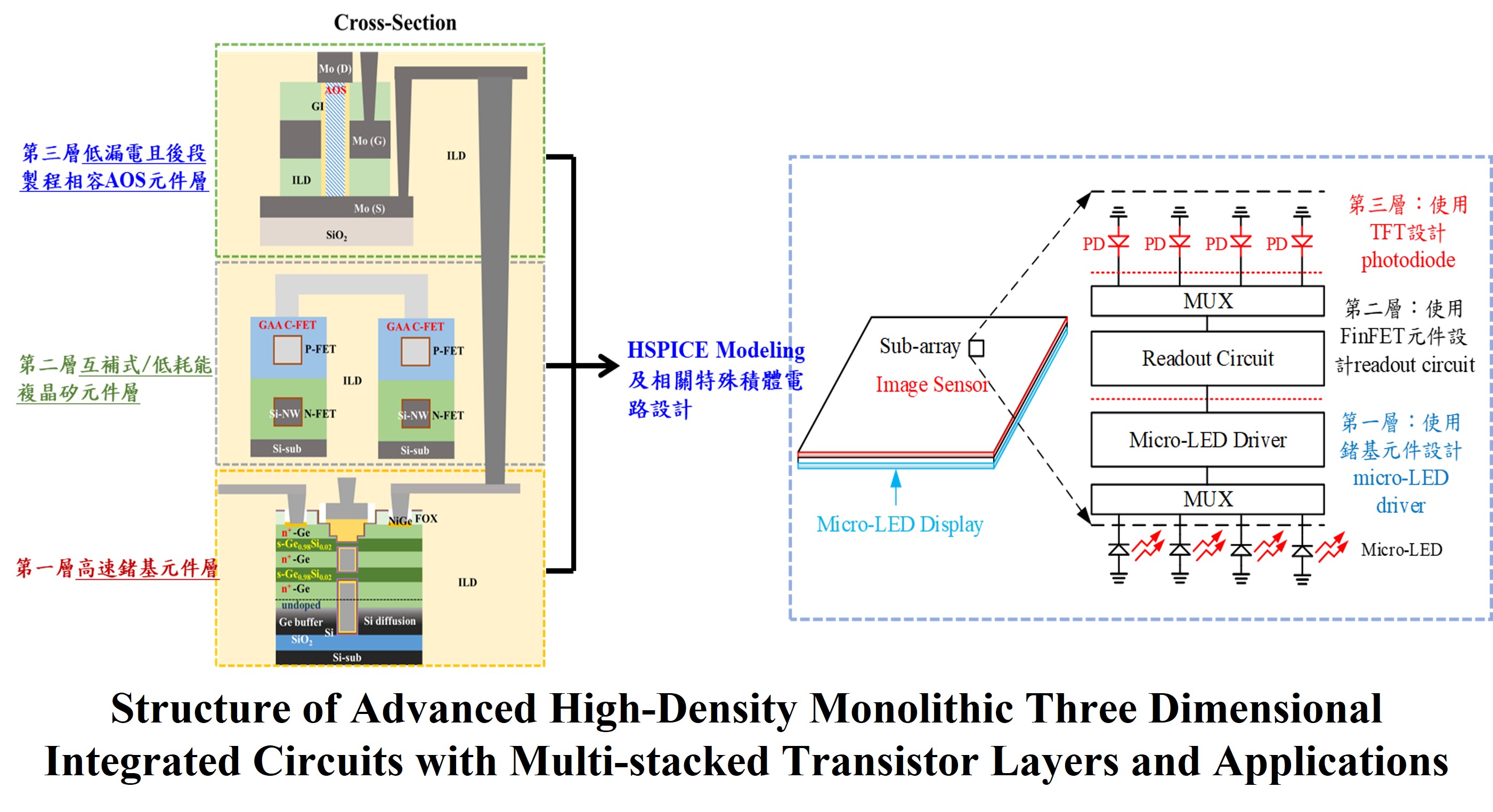
Development for Advanced High-Density Monolithic Three Dimensional Integrated Circuits with Multi-stacked Transistor Layers
World Leading High Aspect Ratio Digital Lithography & High Taper angle Sputtering Technologies
.png)
Smart measurement system for advanced PCB with high speed and high frequency requirements Innovative technology for HPC 5G and High Power Filed
Technology maturity:Trial production
Exhibiting purpose:Product promotion、Display of scientific results
Trading preferences:Exclusive license/assignment
Coming soon!