
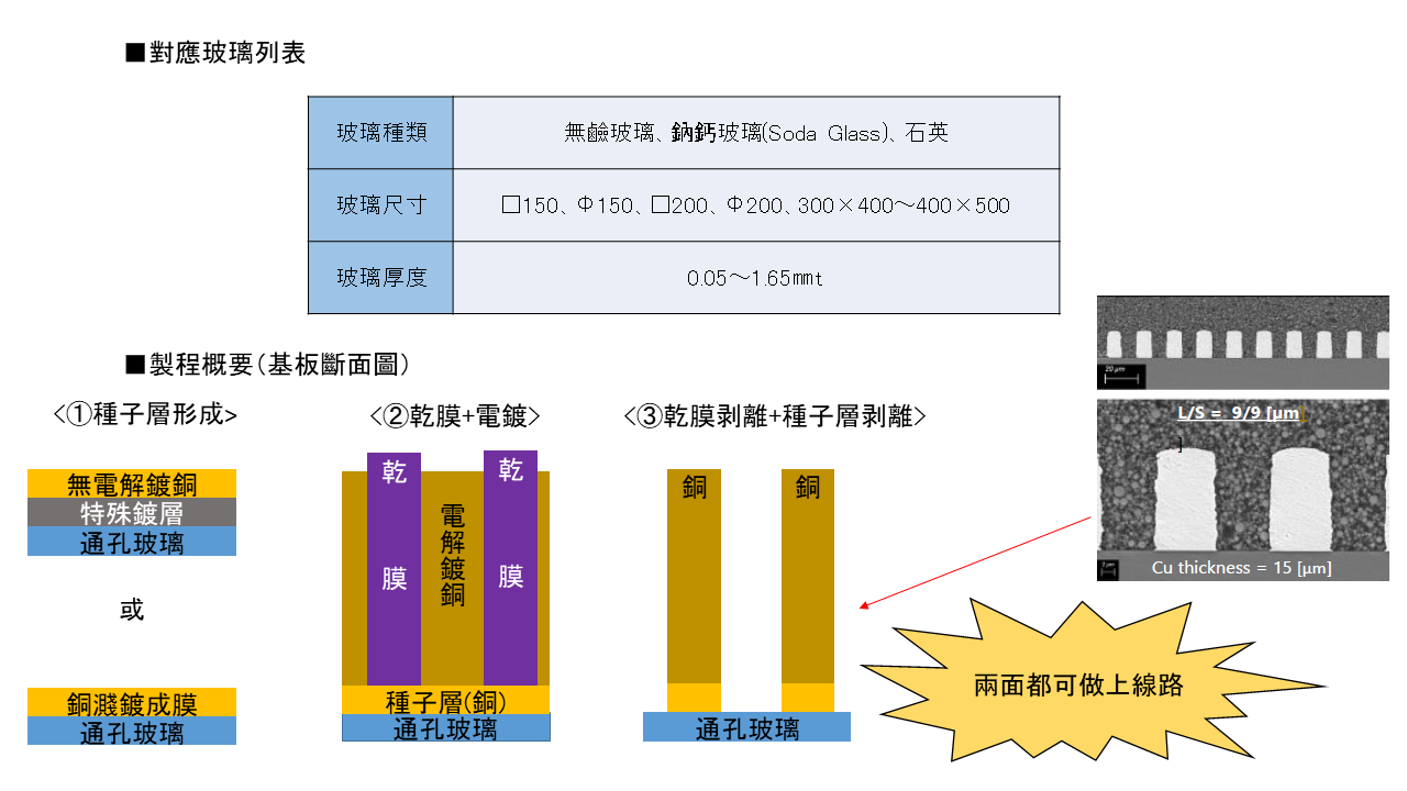
Thickness: 0.2mm or more / Hole diameter: Φ20μm or more
Double-sided wiring/multilayer wiring
(Example) L/S: 3μm
Micro LED electrode
Organic EL transfer electrode
glass interposer
For PCB mounting
through glass Via TGV,film eching
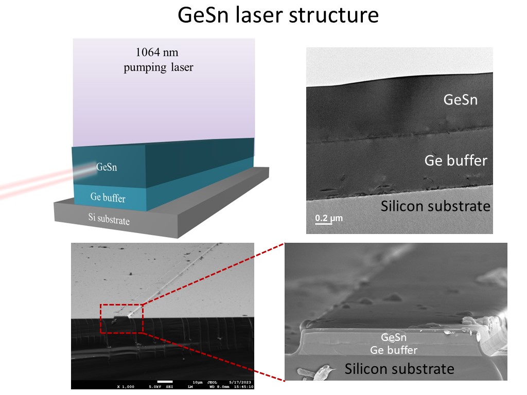
Key enabling light source technology for silicon photonics: Group-IV laser s monolithically integrated on silicon
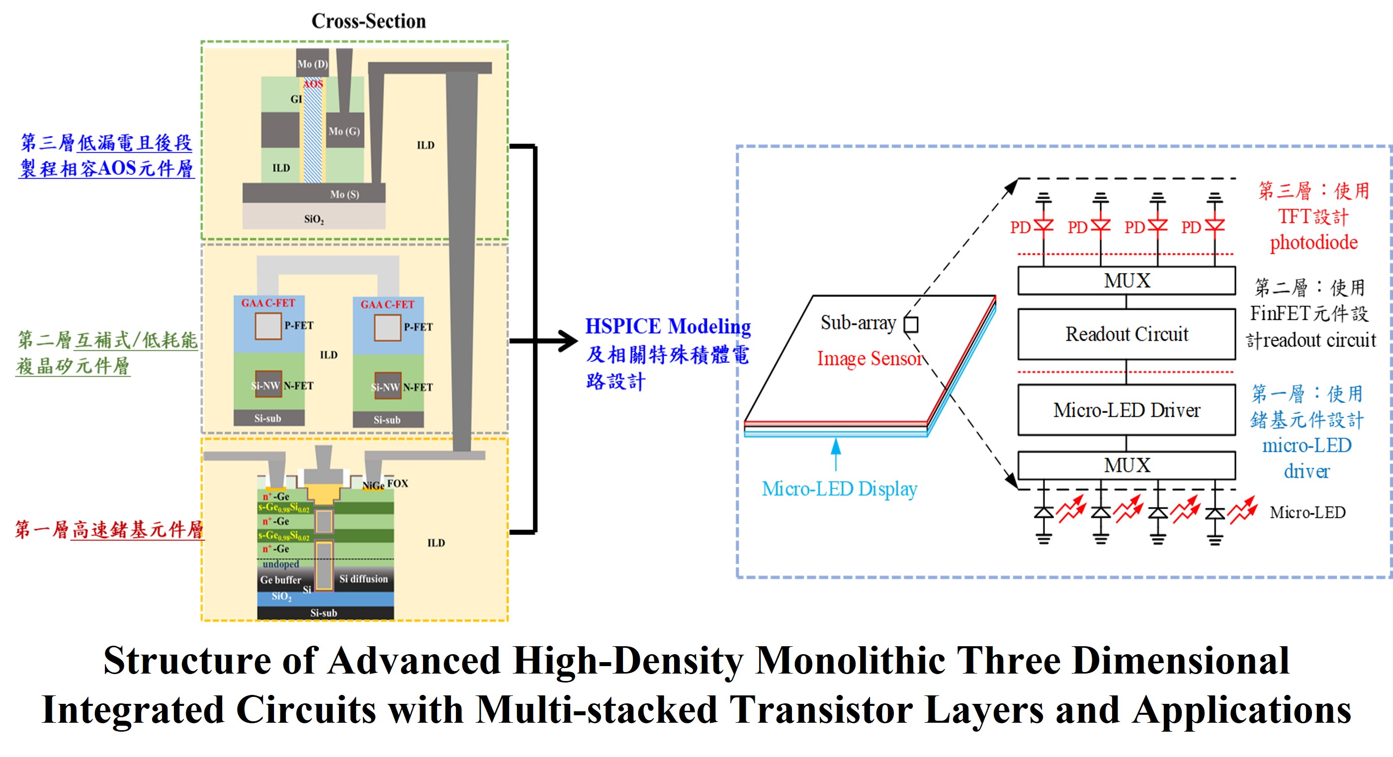
Development for Advanced High-Density Monolithic Three Dimensional Integrated Circuits with Multi-stacked Transistor Layers
Hybrid CMOS Inverter Comprised of Thin Film Transistors with Hetero-channel for Monolithic 3D-ICs and Ultra-high Resolution Flat-Panel Displays Applications
Low Temperature Polycrystalline Silicon Oxide (LTPO) TFT Architecture with Memory-embedded in Pixel for High-resolution and Power-saving Near-eye VR/AR Displays Applications
Technology maturity:Mass production
Exhibiting purpose:Product promotion
Trading preferences:New products development、Negotiate by self
Coming soon!