Feasible Technology for graphene application in electronic Interconnections

This technology consists of two parts. Part 1 is the low temperature PVD graphene deposition process on copper interconnections, and part 2 is the method of embedding graphene inside copper interconnections to ease the subsequent interconnects backend processes, while keeping the interconnect resistivity low, high thermal conductivity and electromigration reliability through the embedded graphene. This method is an addition of 10 minutes immersion of the copper interconnects with graphene on top in copper sulphate solution. The method can also be used for Al interconnections.
As graphene can be patterned using conventional etching process, Al interconnections will be much easier. Since the conduction is through the graphene, the issues associated with Al will not be a problem.A low temperature graphene deposition on VLSI interconnections for backend process compatibility and a method of embed this graphene in VLSI interconnections so that standard mature interconnection processes can be applied. Electrical and thermal conductions will be via the embedded graphene which are excellent as compared to any metals, and electromigration reliability of such interconnect is also proven to be at least three time higher in lifetime as compare to copper.This technology can be used for all interconnects in both integrated circuits and printed circuit boards. The cost of this technology is low because it only requires an immersion tank of copper sulphate solution. Our technology uses a PVD process based on amorphous carbon, so graphene (Gr) deposition on interconnects can also be low temperature and cost-effective.
With Gr alone on copper, the thermal and electrical properties are greatly improved, and its electromigration life is also increased by at least three times, as shown in our experimental results. The technology can also be applied to other metal interconnects. Good interconnections are essential to all electronic circuits, this technology can make an important contribution in the electronics industry.
Name:林宜慧
Phone:03-2118800#3872
Address:259 Wen-Hwa 1st Road, Kwei-Shan Tao-Yuan,Taiwan,333, R.O.C.

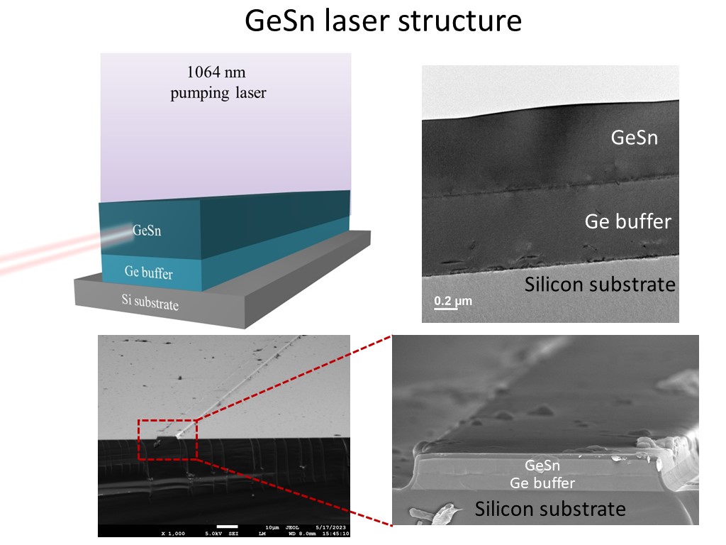
Key enabling light source technology for silicon photonics: Group-IV laser s monolithically integrated on silicon

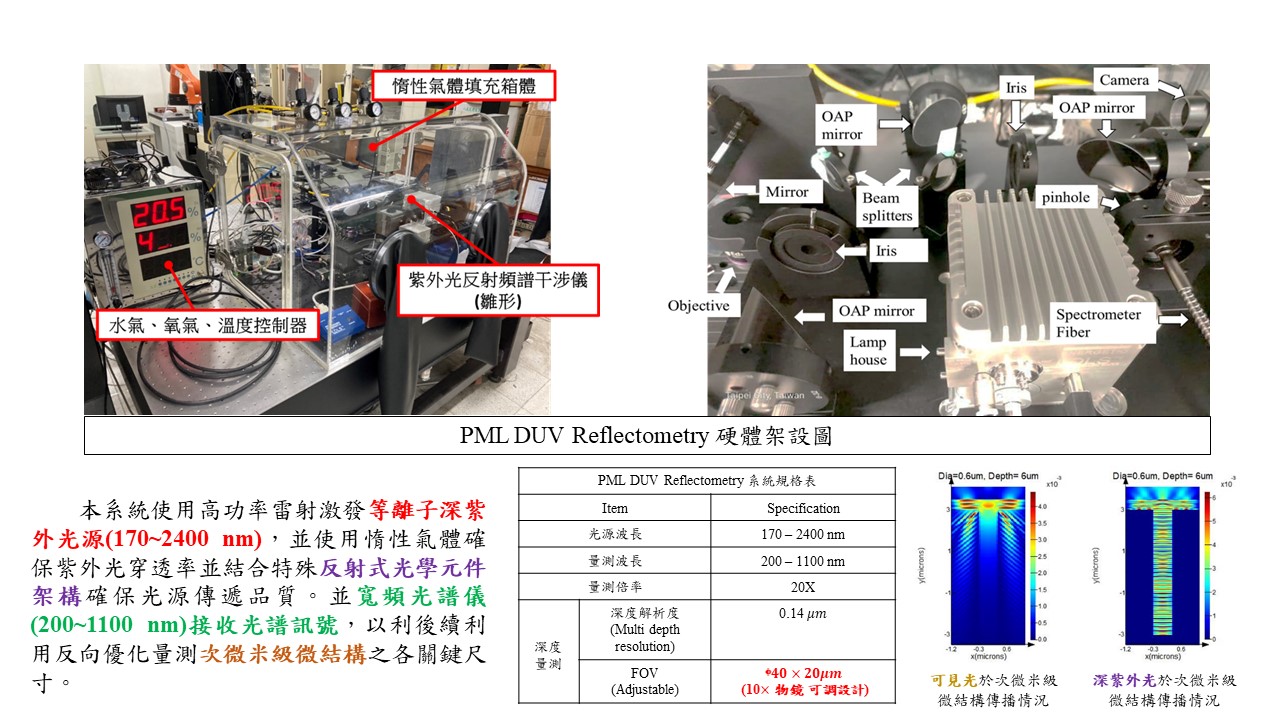
Optical critical-dimension measuring technology for high-aspect-ratio microstructures in advanced semiconductor packaging
Highly Efficient Fabrication and Applications of Bioinspired Flexible Photonic Crystals by Trapping of Structural Coloration

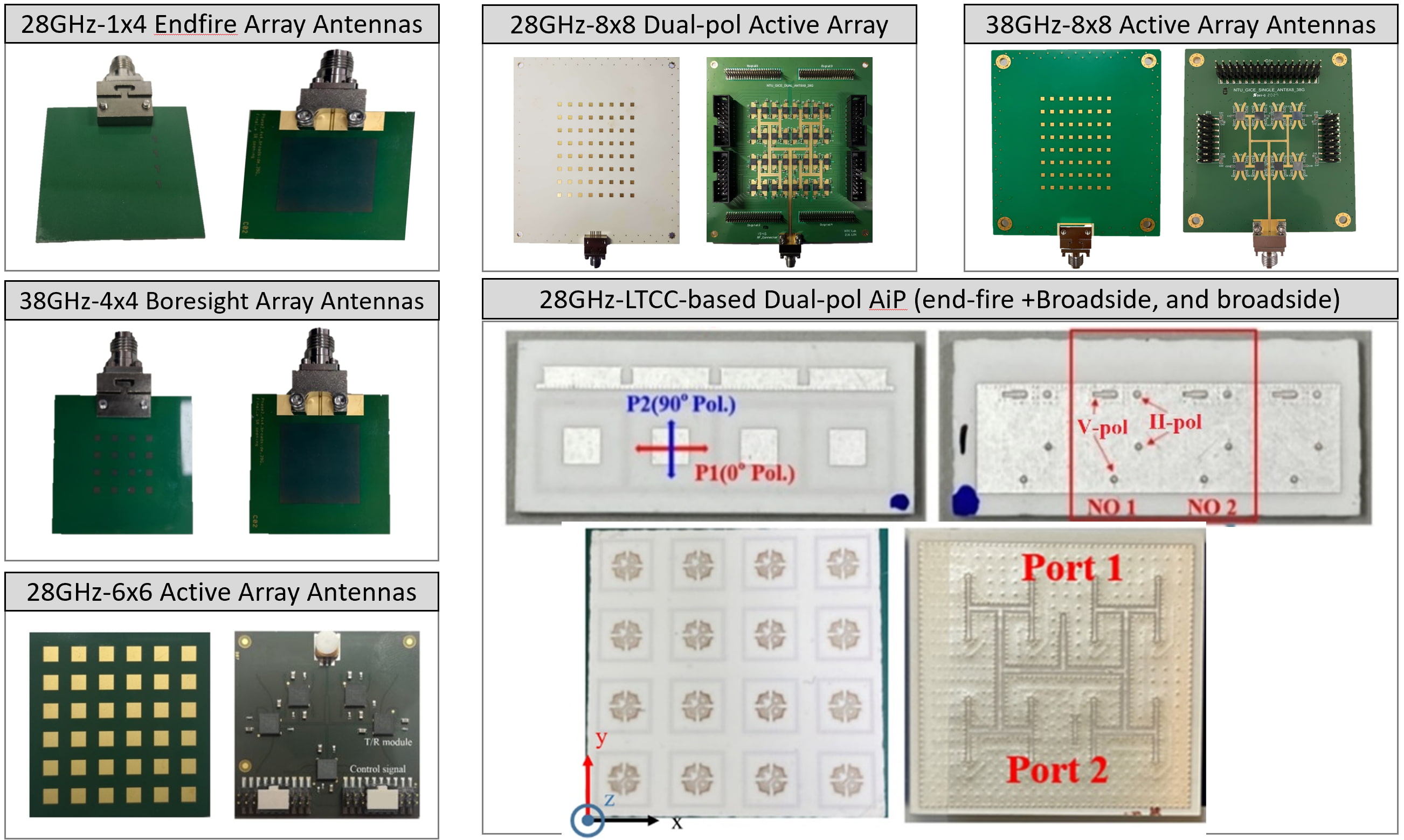
Antenna-in-package (AiP) Technology Suitable for Feeding to the Smart Impedance Material for High-Gain Radiations at Millimeter Wave Frequencies
Technology maturity:Experiment stage
Exhibiting purpose:Patent transactions、Product promotion、Display of scientific results
Trading preferences:Technical license/cooperation、Negotiate by self
*Organization
*Name
*Phone
*Main Purpose
*Discuss Further
*Job Category
*Overall Rating
*Favorite Area
*Key Tech Focus
*Willing to Receive Updates?
Other Suggestions
Coming soon!