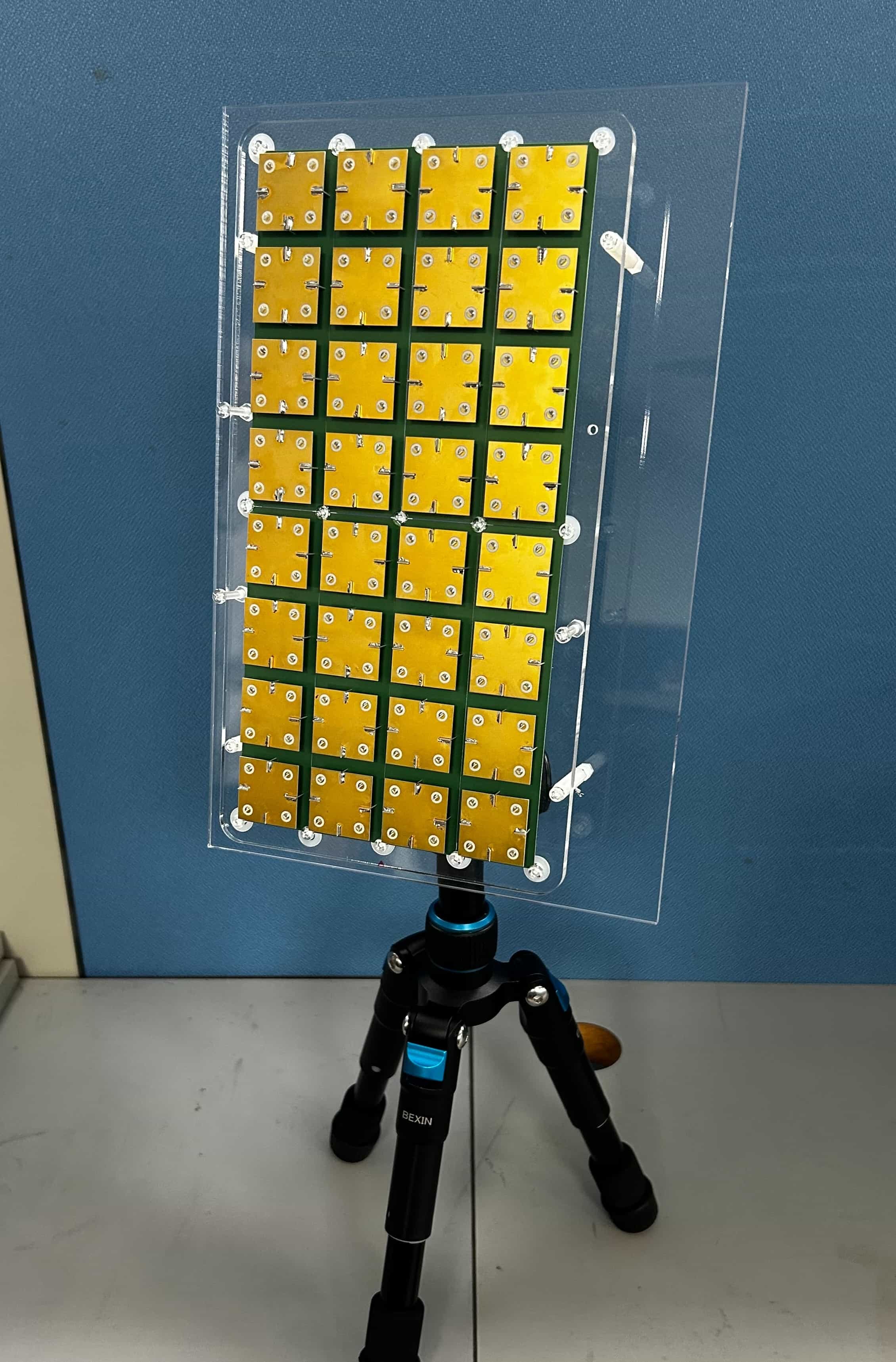
Panel Level Fan-out RDL with Integrated Active/Passive Device Technology
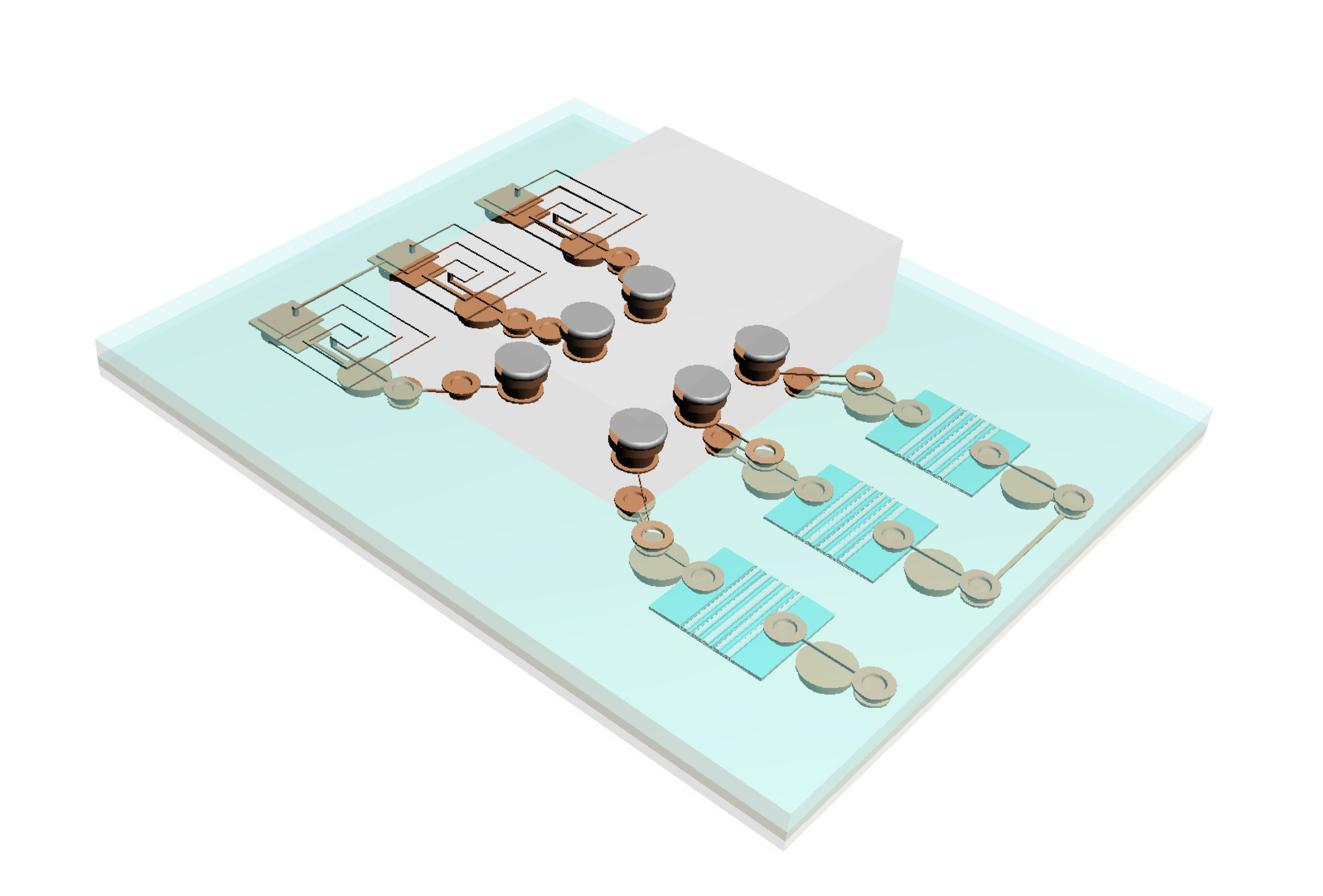
Multiple chips and passive components has been highly integrated by using fan-out packaging technology is a trend, due to the high-end IC packaging developing towards System in Package (SiP). Therefore, this technology combines panel-level redistribution layer (RDL) technology and panel-level thin-film component technology to develop functional RDL interposers that integrate thick-film components (inductors) and thin-film components (capacitors) to become a band pass filter, for radio frequency wireless communications application. The circuit of product can be miniaturized by reducing passive components, and the saved space can be used to the increasing battery volume for improving the endurance of 5G mobile communication products. In addition, in order to prevent the multi-chip package from being damaged by electrostatic discharge during the manufacturing process. In the IC design, the ESD protection circuit has been usually designed in the chip. In order to achieve more comprehensive protection, the ESD protection circuit is also designed in IC package structure.
This technology develops CDM-ESD (Charged Device Model-Electrostatic Discharge) electrostatic protection circuit through panel-level process and low-temperature polysilicon thin-film transistor (LTPS-TFT) technology to improve ESD protection ability of fan-out panel-level packaging.
This technology reduces the active/passive device thickness by more than 50% compared to traditional ones to meet the design needs of IC package industry. Furthermore, it will transform small and medium-sized display panel production lines into IC packaging services providers, and help to get into the high value-added package application market.
線上展網址:
https://tievirtual.twtm.com.tw/iframe/840a23da-c392-4628-88e7-7a91083571bc?group=f36efffd-9ee6-4962-aa09-72f6797d2449&lang=en
測試
Name:Terry Wang
Phone:03-5912570
Address:No.195, Sec. 4, Zhongxing Rd., Zhudong Township, Hsinchu County, Taiwan (R.O.C.)
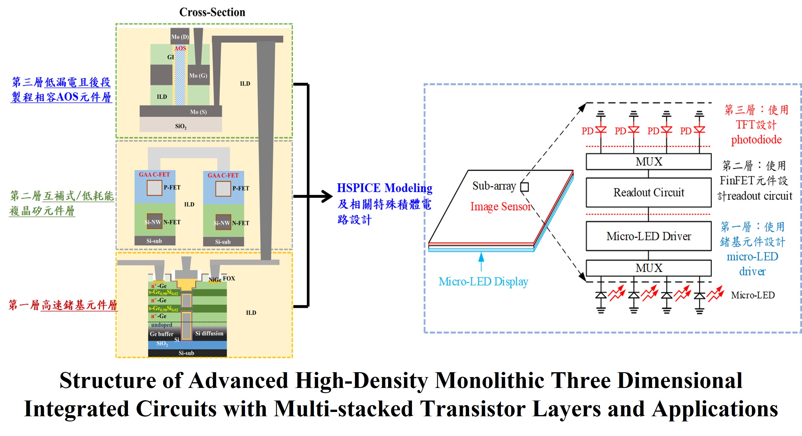
Development for Advanced High-Density Monolithic Three Dimensional Integrated Circuits with Multi-stacked Transistor Layers
Transparent flexible display fabricated by self-emitting quantum dot device and bank-free panel technology
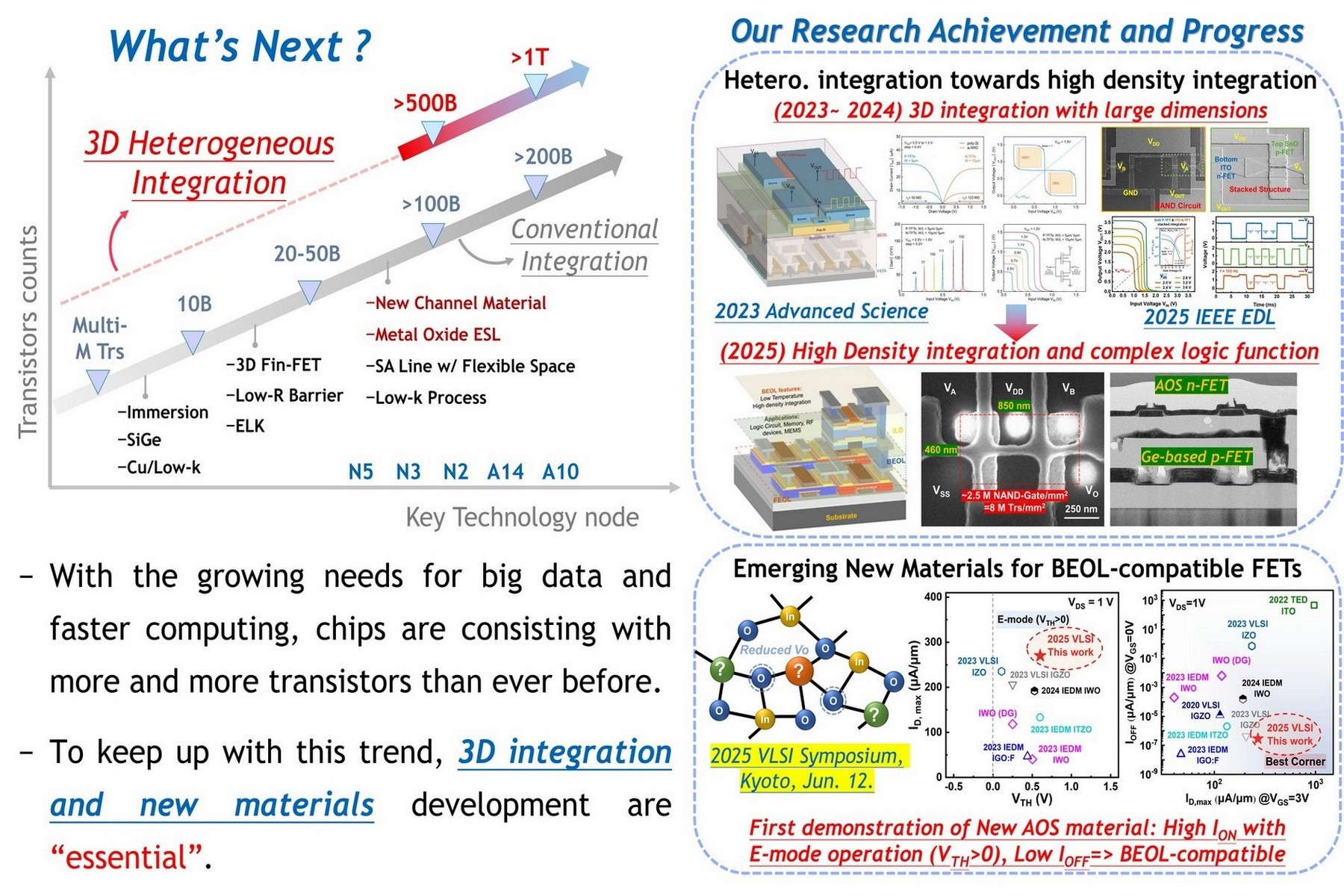
Monolithic 3D Heterogeneous Device Integration and Innovative Materials for Breaking Logic Density Limits: A Key Technology Platform for High-Density AI Computing Chips
6G FR3 RF front-end chipMassive MIMO four-port integrated antenna array technology6G FR3 RF front end module
Technology maturity:Experiment stage
Exhibiting purpose:Technology transactions、Patent transactions、Product promotion、Display of scientific results
Trading preferences:Technical license/cooperation、Negotiate by self
*Organization
*Name
*Phone
*Main Purpose
*Discuss Further
*Job Category
*Overall Rating
*Favorite Area
*Key Tech Focus
*Willing to Receive Updates?
Other Suggestions
Coming soon!