Structured Light Generation and Stereo Vision with All-GaAs Metasurface Holograms
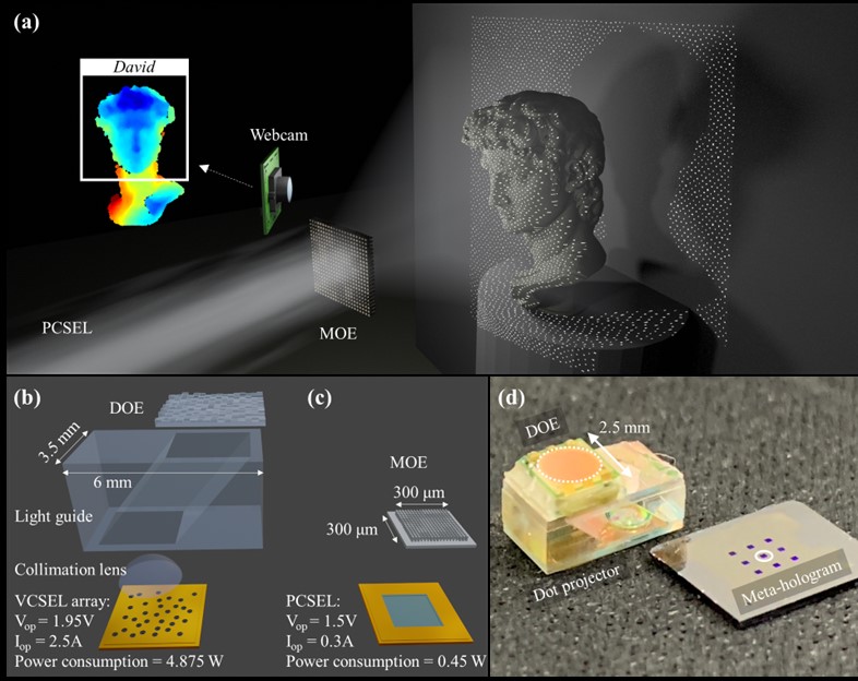
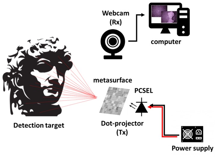
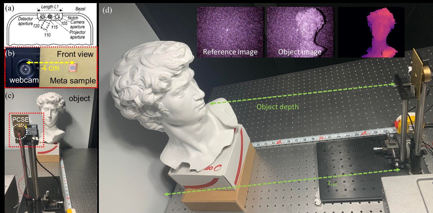
For the first time, we use a single PCSEL as a light source, directly projected onto a designed holo-patterned metasurface. This results in a structure 233 times smaller than an iPhone's, without needing a lens system. This architecture, homogeneously integrated with photonic crystal lasers, reduces power consumption by 10.8 times compared to conventional systems. This innovation achieves miniaturization, lightweighting, and energy saving, making it easier to integrate into AR/VR systems.
National Yang Ming Chiao Tung University (NYCU) was formed in 2021 through the merger of National Yang Ming University and National Chiao Tung University. Located in Hsinchu, Taiwan, NYCU is a leading institution specializing in technology, engineering, medicine, and social sciences. The university is known for its strengths in research and innovation, particularly in areas such as information technology, biomedicine, and artificial intelligence. NYCU fosters interdisciplinary collaboration, global partnerships, and aims to nurture professionals with strong academic foundations and leadership skills to address societal challenges and contribute to technological advancements.
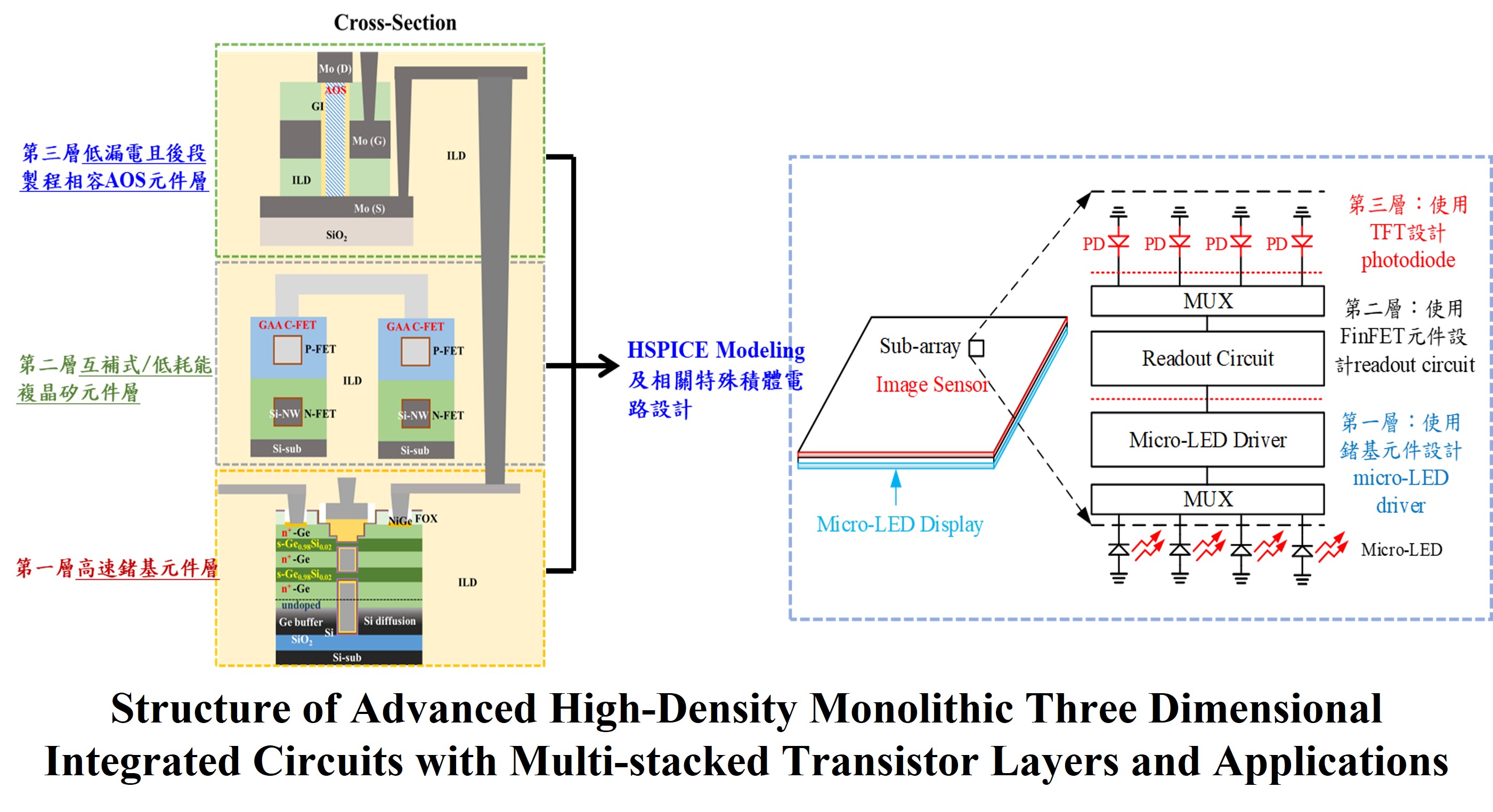
Development for Advanced High-Density Monolithic Three Dimensional Integrated Circuits with Multi-stacked Transistor Layers
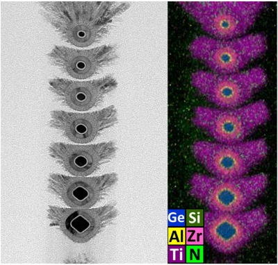
High mobility materials, process, stacked channels, and thermal circuit simulation; Ferroelectric X:HfO2 for Negative Capacitance and POC(Proof-of-Concept) Applications; Atomic layer technologies for
Structural Colors Mini Pixels Enabled by on Silicon Nitride Metasurfaces
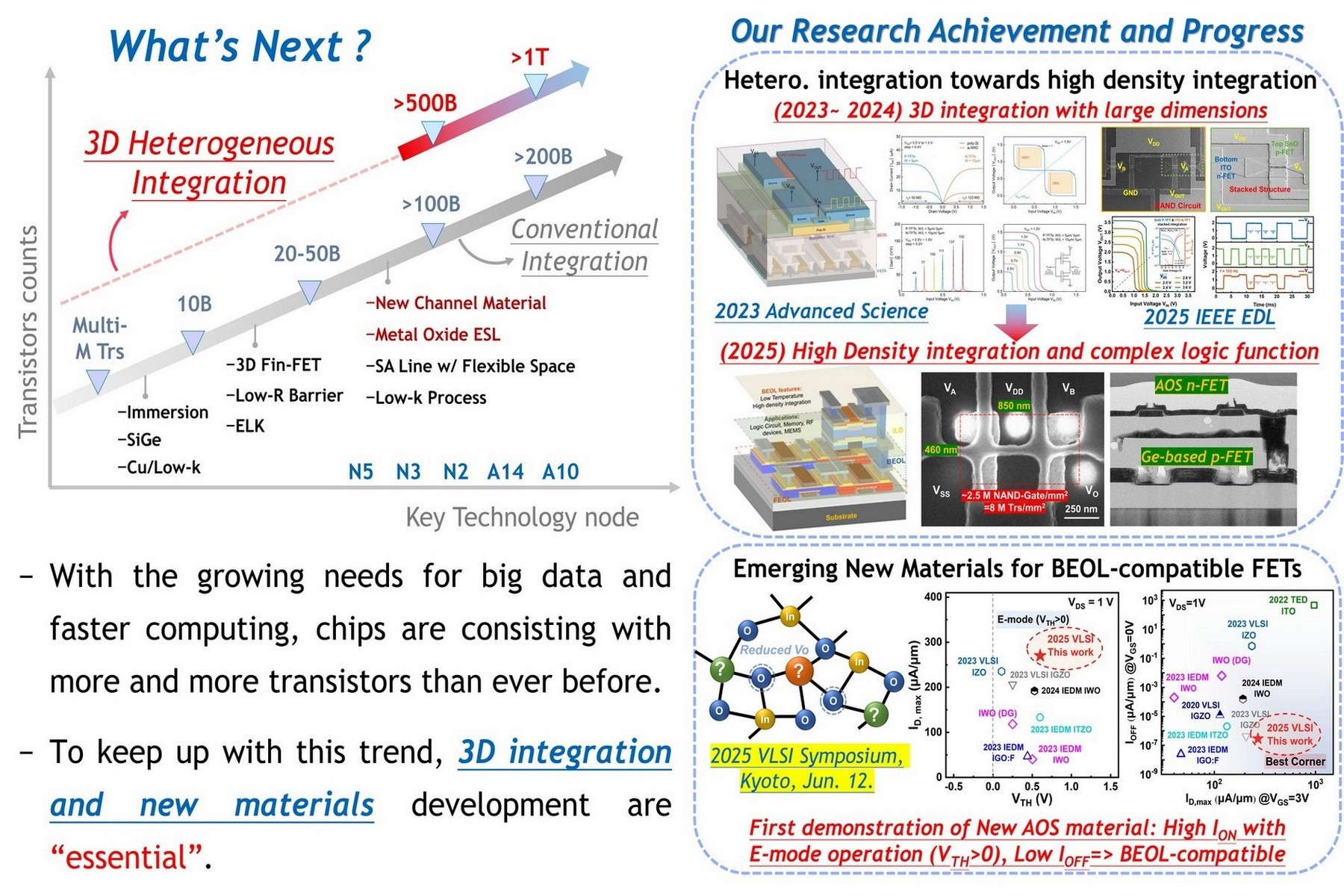
Monolithic 3D Heterogeneous Device Integration and Innovative Materials for Breaking Logic Density Limits: A Key Technology Platform for High-Density AI Computing Chips
Technology maturity:Prototype
Exhibiting purpose:Display of scientific results
Trading preferences:Negotiate by self
*Organization
*Name
*Phone
*Main Purpose
*Discuss Further
*Job Category
*Overall Rating
*Favorite Area
*Key Tech Focus
*Willing to Receive Updates?
Other Suggestions
Coming soon!