Smart Power-saving Display Pixel Array Technology with Low Latency Applicable for AR/VR Wearable Devices
A power-saving memory-in-pixel (MIP) display technology was proposed, in which an innovative CBRAM memory was embedded in a display pixel to provide the image signal to the pixel, especially in a static display period, instead of repeatedly feeding it from the peripheral drivers. In addition to the power-saving, the MIP integrated with the TFT array can increase the pixel aperture ratio compared with SRAM-embedded architecture, and decrease the layout area of peripheral drivers. Furthermore, the high-conductivity copper wiring as electrodes and interconnects was integrated into the TFT backplane array, which can enhance the speed of signal transmission and reduce the image delay, beneficial for high-resolution VR/AR device applications.
National Yang Ming Chiao Tung University (NYCU) was formed in 2021 through the merger of National Yang Ming University and National Chiao Tung University. Located in Hsinchu, Taiwan, NYCU is a leading institution specializing in technology, engineering, medicine, and social sciences. The university is known for its strengths in research and innovation, particularly in areas such as information technology, biomedicine, and artificial intelligence. NYCU fosters interdisciplinary collaboration, global partnerships, and aims to nurture professionals with strong academic foundations and leadership skills to address societal challenges and contribute to technological advancements.
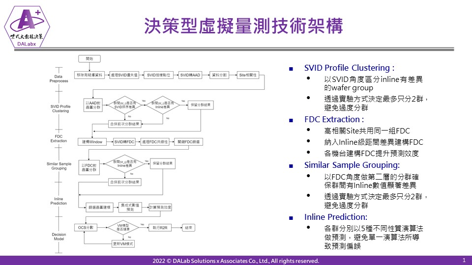
Optimizing Advanced Process Control Decision and Virtual Metrology Technology for Nano Technology Nodes for Semiconductor Manufacturing
.png)
Smart measurement system for advanced PCB with high speed and high frequency requirements Innovative technology for HPC 5G and High Power Filed
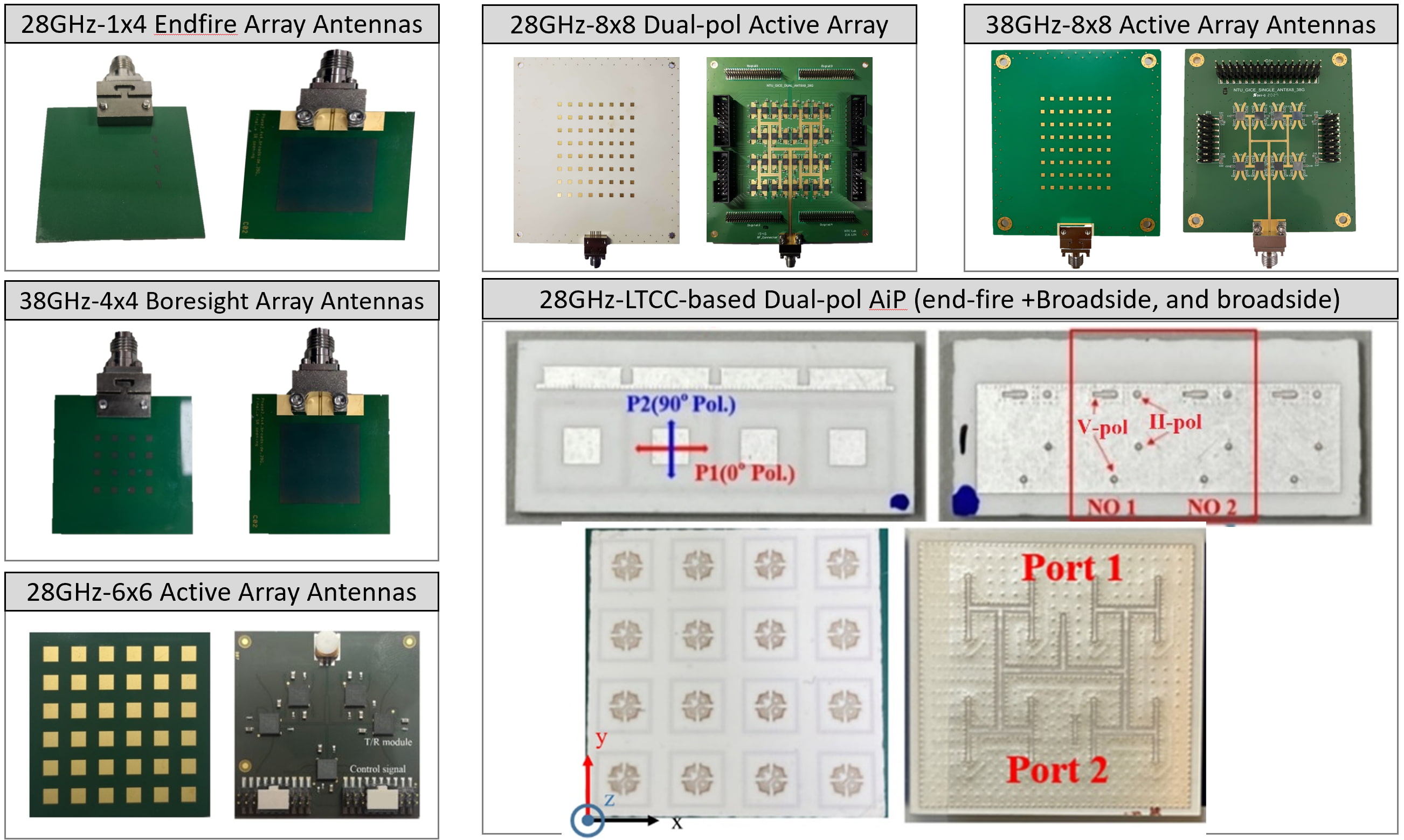
Antenna-in-package (AiP) Technology Suitable for Feeding to the Smart Impedance Material for High-Gain Radiations at Millimeter Wave Frequencies
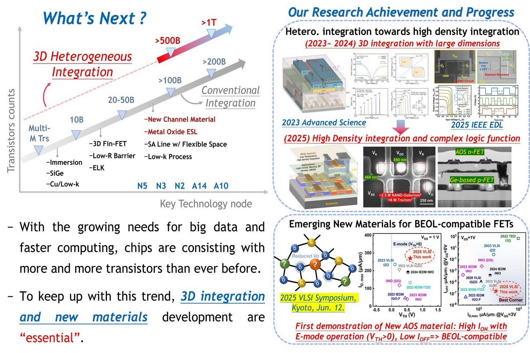
Monolithic 3D Heterogeneous Device Integration and Innovative Materials for Breaking Logic Density Limits: A Key Technology Platform for High-Density AI Computing Chips
Technology maturity:Experiment stage
Exhibiting purpose:Display of scientific results
Trading preferences:Exclusive license/assignment、Technical license/cooperation、Negotiate by self
*Organization
*Name
*Phone
*Main Purpose
*Discuss Further
*Job Category
*Overall Rating
*Favorite Area
*Key Tech Focus
*Willing to Receive Updates?
Other Suggestions
Coming soon!