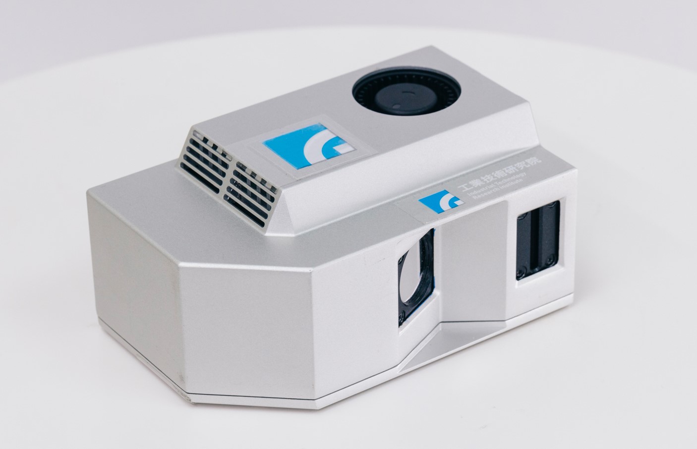
Using the thermal perturbation-resistant depth sensing technology to be the foundation of laser 3D measurement system for transparent surfaces, replace the complicated procedures (spraying、measuring and cleaning) required by the existing AOI 3D measurement technology. Significantly shorten more than 95% of the measurement time (original 60 minutes was shortened to 1.5 minutes), and can implement quality control processes on the production line.
測試
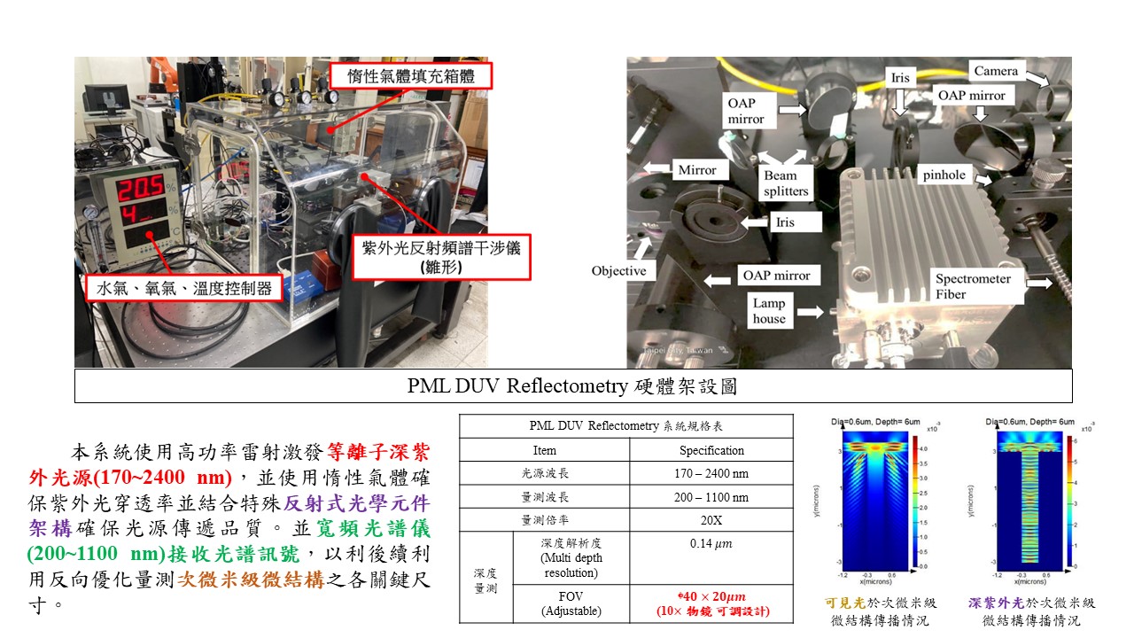
Optical critical-dimension measuring technology for high-aspect-ratio microstructures in advanced semiconductor packaging
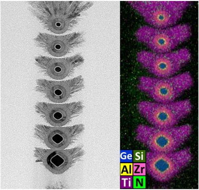
High mobility materials, process, stacked channels, and thermal circuit simulation; Ferroelectric X:HfO2 for Negative Capacitance and POC(Proof-of-Concept) Applications; Atomic layer technologies for
.png)
Smart measurement system for advanced PCB with high speed and high frequency requirements Innovative technology for HPC 5G and High Power Filed
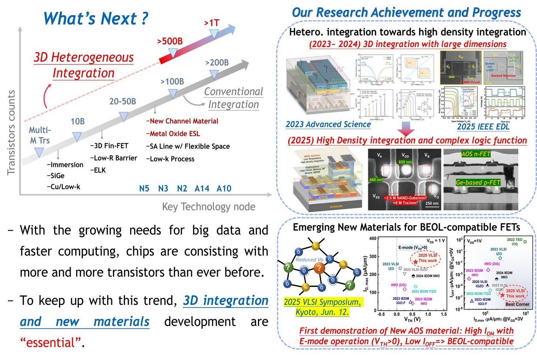
Monolithic 3D Heterogeneous Device Integration and Innovative Materials for Breaking Logic Density Limits: A Key Technology Platform for High-Density AI Computing Chips
Technology maturity:Trial production
Exhibiting purpose:Technology transactions、Patent transactions、Product promotion、Display of scientific results
Trading preferences:Technical license/cooperation、Negotiate by self
*Organization
*Name
*Phone
*Main Purpose
*Discuss Further
*Job Category
*Overall Rating
*Favorite Area
*Key Tech Focus
*Willing to Receive Updates?
Other Suggestions
Coming soon!